This thread has been locked.

If you have a related question, please click the "Ask a related question" button in the top right corner. The newly created question will be automatically linked to this question.

TMS320C6678: About SRIO Boot

Part Number: TMS320C6678

Hello,

I`m trying to understand exact way for SRIO booting on C6678. I read bootloader user guide and my current understanding is below:

  • User`s application code for SRIO booting can`t use RBL`s work area for any 'initialized section'. But user can still put 'uninitialized section' on that area.
  • If users want to use DirectIO mode for SRIO booting, the host must know DSP`s memory map exactly. Host must write required memory image into target device memory space via SRIO direct IO.
  • Once required image has been written, host must write address information for entry point (in most case, c_int00) into MAGIC address. During SRIO booting, RBL keeps polling MAGIC address and branches to it once it is non-zero value. And then, application starts its execution (on core0)

First of all, please let me confirm my understanding is correct.

And the following is my questions;

1. Bootloader user guide says there is 32KB for RBL workspace, but i can`t understand exact address. 

2. I`m now reading BootROM_C6678_PG2.0\BootROM_c6678_PG2.0\main\riomain2.c for my understanding. I believe the following is core loop for waiting MAGIC.

do  {


    /*---------------------  SRIO direct write boot mode processing ------------------ */

#ifdef BOOTCONFIG_INCLUDE_RAPIDIO_BTBL

    if ((origOptions & BOOT_PARAMS_RIO_OPTIONS_BOOT_TABLE) == 0)  {

#endif

/*  */

/*  */
/*  */
/*  */
/*  */

	  } else {

        /* Wait for the rapid I/O interrupt */
        chipSleepUntilEvent ((UINT16)DEVICE_SLEEP_RIO_EVENT);
	  } 

      /* Clean up after the rio interrupt */
      hwRioCleanup ();

      /* Peform any table processing (emif config tables, peripheral config tables, etc) */
      chipRioBlockDone ();

#ifdef BOOTCONFIG_INCLUDE_RAPIDIO_BTBL

    /*-------------------  SRIO message mode (boot table) processing --------------------- */

    }  else  {

      /* In case direct write boot is used with the boot table bit set (the default),
       * poll the ifr bit. If set check to see if DDR setup was setup */
      if (chipPollIfr (params->portNum, DEVICE_SLEEP_RIO_EVENT) == TRUE)  {
        hwRioCleanup ();
        chipRioBlockDone ();
      }


      pkt = chipSrioGetPkt(&vcppi, &len);

      if (vcppi != NULL)  {

          status = boot_rio_table_proc (pkt, len);

          if (chipSrioPktDone (vcppi) != 0)  {
            bootStats.u.rapidIo.rapidIoDescrEmpty += 1;
            chipStatusRioDescrEmpty();
          }

          if (status == RIOMEM_LENGTH_READY_LENGTH_INVALID)  {
            bootStats.u.rapidIo.rapidIoBtblBadBlocks += 1;
            chipStatusRioBadLength ();
      
          } else if (status == RIOMEM_LENGTH_READY_CHKSUM_FAIL)  {
            bootStats.u.rapidIo.rapidIoBtblBadBlocks += 1;
            chipStatusRioBadChksum ();

          } else  {
            bootStats.u.rapidIo.rapidIoBtblBlocks += 1;
            chipStatusRioBtbl ();

         }

         /* Peform any table processing (emif config tables, peripheral config tables, etc) */
         chipRioBlockDone ();

      }

   }


#endif

  } while ( !(*p_boot_entry_addr) );


Now no definition for BOOTCONFIG_INCLUDE_RAPIDIO_BTBL, so most of the code is not activated in RBL. so now it should look like this :

   do  {


    /*---------------------  SRIO direct write boot mode processing ------------------ */

/*  */

/*  */
/*  */
/*  */
/*  */

	  } else {

        /* Wait for the rapid I/O interrupt */
        chipSleepUntilEvent ((UINT16)DEVICE_SLEEP_RIO_EVENT);
	  } 

      /* Clean up after the rio interrupt */
      hwRioCleanup ();

      /* Peform any table processing (emif config tables, peripheral config tables, etc) */
      chipRioBlockDone ();

  } while ( !(*p_boot_entry_addr) );


...As you see, c-scope is inconsistent. Can you share the corrected do-while for my reference ?

Sorry, I don`t know exact SRIO specification ... so my poor question starts from here :-(

3. If I understand RBL code correctly, during RBL process, the node id (device id ?) seems to be 0xFFFF by default. Does this mean DSP can accept any incoming packets having any destination id ?

4. If SRIO switch is present between HOST and DSPs, how does host select target DSPs (having same node id as 0xFFFF) for downloading the image ? If host configures SRIO switch to route the packet to dedicated output port for a target DSP, and send packets with any device ID, the slave DSP can accept incoming packets ?

5. If a single application image is running on core0-7, how to run core1-7 after SRIO booting ? Let`s assume all cores are sharing the code on MSMC SRAM and some local sections dedicated for each core are present on L2 local address. In this case, I`m wondering if the following scheme can work for me. Is that correct ?

  - Host is holding DSP boot table image. Host downloads each sections into DSP via SRIO DirectIO by parsing boot table format. During this process, it can detect initialized sections dedicated for L2 local address and host can convert them from LOCAL to GLOBAL address and download them for ALL cores. As for shared sections on MSMC SRAM, host just download it as is. After boot process is completed successfully, only core0 application starts working and it has to generate IPC interrupts for each of the secondary CorePacs to awake. Then secondary cores (core1-7) starts their execution. 

Sorry for many poor questions but I have some customers to use SRIO booting , so I want to exact way. It would be appreciated if you could answer to my questions. Thank you !!

Best Regards,
Naoki

  • Hi Naoki,

    I've forwarded this to the SRIO experts. Their feedback should be posted here.

    BR
    Tsvetolin Shulev
  • Hello,

    Do you have any update on this ? I`m waiting for your reply.

    Best Regards,
    Naoki
  • Naoki,

    Here is a short summary of responses to your questions:

    For details of 32KB in L2 memory refer section 2.4 in datasheet:
    www.ti.com/.../tms320c6678.pdf

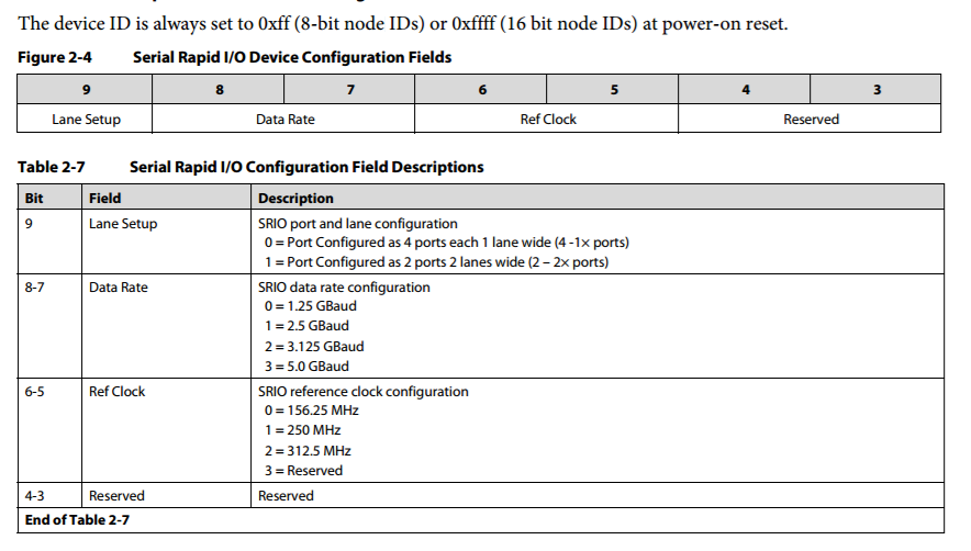
    The device ID is always set to 0xff (8 bit node IDs) or 0xffff (16 bit node IDs) for booting from SRIO through pin strapping. Any value can be used when using a two stage SRIO boot and is specified through the boot parameter table.

    SRIO ROM boot details:
    --------------------------------

    The ROM initializes the SRIO sub-system. In SRIO boot mode the message mode will be enabled by default. If message mode has been disabled (from the boot parameter table) then the ROM code executes an idle. Message mode can only be disabled in a two stage boot. The default boot parameter table constructed from pin values will always set message mode enabled.

    If use of the memory reserved for received messages is required, and reception of messages cannot be prevented, the master can disable the message mode by writing to the boot table and re-entering boot. The SRIO is configured to forward all packets through the TLM (promiscuous mode). This is the default setting.

    When the ROM code detects a non-zero value in the boot magic address the boot exit function is executed, and the ROM branches to the value found in the boot magic address.

    To see how SRIO boot on C667x works on EVM, please look at the e2e post her:
    e2e.ti.com/.../456577

    We provide a SRIO boot example that also demonstrates waking up secondary cores. This example is provided in the Processor SDK RTOS that you can locate here:
    processors.wiki.ti.com/.../Processor_SDK_RTOS_BOOT_C66x


    Regards,
    Rahul
  • Hello Rahul,

    Thank you so much for your answer. I`ll check your example code later, but in HW perspective, I need further clarification about this

    Rahul Prabhu said:
    For details of 32KB in L2 memory refer section 2.4 in datasheet:
    www.ti.com/.../tms320c6678.pdf

    I read this chapter, but I could not find the 32KB size of reserved memory segment. Did you mean 32KB reserved area was from 0x00872DC0 to 0x0087FFFF ? It is not 32KB.

    Rahul Prabhu said:
    he device ID is always set to 0xff (8 bit node IDs) or 0xffff (16 bit node IDs) for booting from SRIO through pin strapping.

    I could not find the dedicated boot strap pin for this selection. Can you clarify ?

    Best Regards,
    Naoki

  • Hi,

    Any response ? I`m sorry to rush you, but I need to visit the customer tomorrow.

    Best Regards,
    Naoki
  • The following region in L2 memory is used for the SRIO messages:  

    Here are the bits in DEVSTAT (BOOTMODE[15:0]) that are used for the node IDs

    If it is 2 lane then the node ID is 0xFF and if it is 4 lane then it is oxFFFF

  • Rahul,

    Thanks for your reply, but as for node ID, The ROM code does not say so;

    Here is a snippet from rom code (rev2.0) and it initializes the boot parameter table on POR.

    void bootInitBootParamsRapidIo (BOOT_PARAMS_RIO_T *params)
    {
    UINT32 pll;

    params->boot_mode = BOOT_MODE_RAPIDIO;
    params->length = (UINT16) (CHIP_WORDS_TO_BYTES(sizeof(BOOT_PARAMS_RIO_T)));
    params->checksum = 0;
    params->portNum = chipGetDefaultRapidIoPortNum ();

    pll = chipGetDefaultRapidIoPll ();
    params->swPllCfg_msw = chipUpper16 (pll);
    params->swPllCfg_lsw = chipLower16 (pll);

    /* */
    /* */
    /* */
    params->options = chipGetDefaultRapidIoOpts_NonSec (); /* non-secure device use master mode as default */
    /* */

    params->lane_port_setup = chipGetDefaultRapidIoLanePortSetup ();
    params->cfg_index = chipGetDefaultRapidIoIndex ();
    params->node_id = chipGetDefaultRapidIoNodeId ();

    chipGetDefaultRapidIoSetup(&params->serdes_ref_clk, &params->link_rate);

    params->pf_low = chipGetDefaultRapidIoPfLow ();
    params->pf_high = chipGetDefaultRapidIoPfHigh ();

    } /* bootInitBootParamsRapidIo */

    The above red code sets params->node_id to 0xFFFF.  chipGetDefaultRapidIoNodeId() is defined like this;

    #define chipGetDefaultRapidIoNodeId()       0xffff

    You say BOOTMODE[9](lane setup, 4-1x port or 2-2x port) is related to node id, but it seems this part is related to the above blue code. No relation ship for node_id. Can you clarify ?

    Best Regards,
    Naoki

  • Hi,

    I'm waiting for your reply.
    Thank you in advance.

    Naoki
  • Hi,

    What is the answer for this ?

    Naoki
  • Hi,

    What is the answer for this ? My customer is waiting for your reply.

    Also, my understanding is any 1x port can accept incoming boot image from the SRIO host device if we setup BOOTMODE[9] as 0. Correct, right ?

    Regards,
    Naoki
  • Your understanding is correct the BOOTMODE[9] relates to chipGetDefaultRapidIoLanePortSetup and not the Node Setup. The SRIO NodeId is always set to 0xffff by the boot ROM. unless an alternate Boot parameter table with different Node ID is provided.

    1x port can accept incoming boot image from the SRIO host device if we setup BOOTMODE[9] as 0.
    Yes, the 4 lanes can be used together or individually so any 1X port can can accept incoming data.
  • Thanks for your reply. Ok, understand. I close the thread.

    Best Regards,
    Naoki