


Other Parts Discussed in Thread: TMDXSK437X
Hi all,
I have some questions about TMDXSK437X schematic.
My Reference document
SCH : am437x_starterkit_evm_3k0009.dsn
DS : SPRS851D.PDF
UG : SPRUHW8.PDF
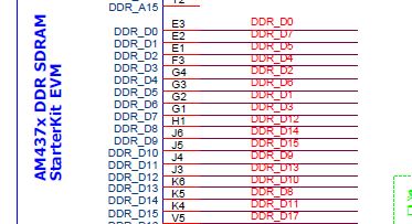
Q1.
DDR_D 0 to DDR_D 31 of SCH and PIN NAME of DS are different.
Is this a typo of SCH?
Q2.
The AE10 pin of SCH is open, but in DS this is described as VSS pin.
Should this pin be connected to GND?
Q3.
The AA23 pin of SCH is TEST_EN, but in DS this is described as VSS pin.
Is this a typo of SCH?
Q4.
The AE7 pin of SCH is open and TPM_WAKEUP, but in DS this is described as VSS pin.
Should this pin be connected to GND? Is this a typo of SCH?
Q5.
The AE8 pin of SCH is open and PMU_HIBZ, but in DS this is described as VSS pin.
Should this pin be connected to GND? Is this a typo of SCH?
Q6.
The description of J15 differs between SCH and UG. Which one is correct?
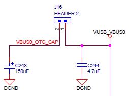
Q7.
When should I use J16 of SCH?
Q8.
What is the power supply specification of the camera module(OV2659) connected to J15?
I am sorry for asking various questions.
Best regards,
Sasaki

