This thread has been locked.

If you have a related question, please click the "Ask a related question" button in the top right corner. The newly created question will be automatically linked to this question.

RTOS/am5728: PCIe benchmarks

Part Number: AM5728
Other Parts Discussed in Thread: SYSBIOS,

Tool/software: TI-RTOS

Hello,

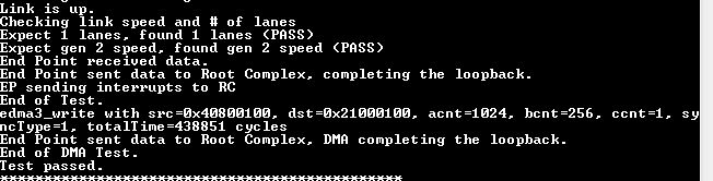
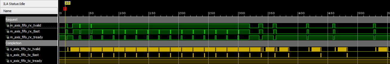
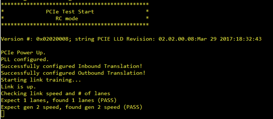
  we're using the 2 PCIe lanes of the am572x to connect to an FPGA in form of a PCIe x2 GEN2 connection. am572x is RC. The configuration and utilisation of the PCIe RC is done on DSP1 core using TI-RTOS with sysbios vers. 6.46.0.23, edma lld vers. 2.12.1 and pcie code derived from the pcie example driver code. The connection works reliable and stable. We see data request TLPs arriving at the FPGA in 64 byte chunks which is a pitty, since to my knowledge at least 128 byte should be possible for the sitara. But even considering the overhead generated by these really small requests we don't achieve the estimated bandwidth.

Our tests show that we only get around half of the theoretical netto bandwidth. If we use only one lane or if we switch to GEN1 instead of GEN2 in both cases the bandwidth drops to nearly half, so we can assume that both features (2 lanes, GEN2) are actually working. We're doing EDMAs from PCIe realm into DSPs L2 RAM or into OCMC RAM. Both result in half of the theoretical netto bandwidth.

Is there some benchmark data we can compare our approach with, to verify our findings and reject possible configuration issues?

Best,

      Tim

  • The RTOS team have been notified. They will respond here.
  • Tim,

    I cannot help with the SW configuration side of this inquiry, but I can confirm that the maximum PCIe outbound payload size for this family of processors (AM57xx) is limited to 64-bytes. The inbound side supports a maximum payload of 256 bytes.

  • Thanks for confirmation - I wasn't sure anymore if it was 128 or 64 bytes outbound.

    Right now I don't have any questions regarding SW configuration, I think I'm fairly familiar with this. What really would help would be any benchmark data I could check against.

  • Hi,

    We have the EDMA+PCIE example in the Processor SDK RTOS AM57x device. As you either change to GEN1 or change to x1 lane, you observed the throughput cut by half. That means you have the PCIE GEN2x2 lane configured right.

    As Dave mentioned, the PCIE outbound size is "Maximum outbound payload size of 64 Bytes (the L3 Interconnect PCIe1/2 target ports split bursts of size >64 Bytes to the into multiple 64 Byte bursts)
    • Maximum inbound payload size of 256 Bytes (internally converted to 128 Byte - bursts)", TRM 24.9.1.1 PCIe Controllers Key Features.

    We don't have benchmarking results on-hand but if you use our RTOS driver I think you can add timer to benchmarking that. You need to exclude the EDMA setup time, the transfer starting point is where you trigger it by writing EDMA ESR register. The finsih point if where EDMA IPR register set. When you use EDMA LLD, there maybe very small overhead.

    In theory, for GEN2X2 the TH is: 5.0Gbps x 2 lane x 8/10 bit encoding * (64 / (64+PCIE TLP header)). The TLP header is about 24-28 bytes depending if 4-byte CRC added or not.

    So, it probably 5.8Gbps = 730 MBps. The real measured number should be closer to this. Let us know what you get for OB write and OB read. If your number is less than half of 730 MBps, we have a problem and need to look at.

    Regards, Eric
  • Good morning,

       thank you for your remarks, Eric. 

    We're using the EDMA LLD and we're measuring the time from the call of EDMA3_DRV_enableTransfer until the ISR function stated at EDMA3_DRV_requestChannel is called with EDMA3_RM_XFER_COMPLETE. The RTOS application consists of the single benchmark task and it tests for the ISR call with a busy loop.

    With this setup we measure a PCIe bandwith for OB 1MByte block read requests of 382MByte/s and for OB 1MByte block write requests of 384MByte/s.

    As you confirmed with your calculation it's roundabout a bit more than half of the estimated bandwidth.

    I am a bit confused by the sentence ' If your number is less than half of 730 MBps, we have a problem and need to look at.' - In our case it's slightly more. Nevertheless this is indeed a problem. We never rely on the full theoretical netto bandwidth in our system designs, but 50% off is a bit too much. We need around 600MByte/s to achieve what we have planned...

    Best regards,

             Tim

  • Tim,

    Thanks for providing the numbers. Yes, it should be closer to 730 MBps. 380 is a problem, I will setup two TI EVM for measurement earilier next week.

    Regards, Eric

  • Hi Eric,

      any numbers?

    Thanx a lot,

                Tim

  • Tim,

    Yes, I did the throughput between two AM572X IDK EVMs connected throughput PCIE cable. Note we only have GEN2x1. In theory half of your bandwidth.

    I used the P-SDK Rel 3.3 PCIE example code, but I think earlier code should have the same results. I ran the test on DSP at 600MHz. I made the following changes:

    1) In   PcieExampleEdmaRC() or PcieExampleEdmaEP(), I simply did a hard coded:

    CCount = 1;

     ACount = 1024;

     BCount = 256;

    Otherwise the EDMA transfer size is controller by PCIE_EXAMPLE_LINE_SIZE. Based on current code, the EDMA destination buffer is in L2 of DSP, which only has 288KB. So my 256KB transfer is good.

    2) I also changed EDMA sync from A-sync to AB-sync edmaTransfer(hEdma,(EDMA3_Type) EDMA_TYPE, (unsigned int*) source, (unsigned int*) remoteBuf,

                  ACount, BCount, CCount, EDMA3_DRV_SYNC_AB,totalTimePointer);

    It is easier for me to set break-point in edma3_test() to see how many cycles spend. Otherwise, there is (i = 0; i < numenabled; i++) loop for me to add up.

    I simply flipped source and destination for EDMA read test. The cycle count for read and write are almost the same (~440000 cycles).

    Below is my number (WRITE case):

    From math: 256 * 1024 /440000 *0.6 = 357MB/s. This is almost the theortical. I don't feel an issue in AM572x. Do you have any way to measure the FPGA to FPGA PCIE throughput?

    Regards, Eric


  • Hi Eric,

      back with some numbers.

    Thanks for doing the test - we were able to 'downgrade' our setup to 1x lane to have comparable results.

    First: there was a fpga bug preventing the underlying RAM-core from delivering maximum bandwidth. With that fixed we were able to substantially increase our read bandwidth. It's now at 285MB/s with 1x lane and around 600MB/s with 2x lanes. Note that with 2x lanes it's a bit more than double the rate with 1x lane.

    This is much better and meets our lowest estimated requirements. But as you state there should be at least 10% more possible...

    Intrestingly if we do a write the Bandwith rises to 345MB/s (1x lane) / 690MB/s (2x lanes).

    I understand the benefit of write requests being posted in contrast to read requests which need a Completion TLP answer. But with TLPs being pipelined and because of the full duplex nature of PCIe this shouldn't take too much of the available bandwidth.

    We did some research on the fpga side and what we see is a stall of read request TLPs from the sitara that limits the bandwidth to 600MB/s. I would like to understand where this stall is coming from.

    On the fpga probe we see 16 request TLPs coming in in a burst. The fpga immediately starts responding from the first TLP on. After 16 request TLPs the time between incoming TLPs gets longer.

    Her one can see in the upper three rows the incoming request TLPs and in the lower three rows the response. Following a description of all signals showing:

    Request

    1. High: there is incoming TLP data pending

    2. High: the last available TLP data is ready to be read

    3. High: the following pipeline is ready to receive the next TLP

    Completion

    1. High: there is outgoing TLP data

    2. High: the last data word of the TLP is ready to be read

    3. High: the transmit side of the PCIe core is ready to read incoming data

    It is obvious that for the first 16 TLPs the FPGA transmit side is stalling (signal m_axis_fifo_rx_tready is low). The first TLP gets handeld immediately but the following are handled with a delay.

    But after these TLPs the incoming TLP fifo dries out (clock cycle 320 in the picture). Now the following pipeline is able to compute the TLPs immediately again. It's waiting most of the time for incoming TLPs.

    Since the PCIe core is 3rd party IP we don't know the implementation details but additionally to the probe in the picture we have done a time correlation via GPIO and we can see that in the beginning the incoming TLP rate is high enough to ensure maximum bandwidth - around 50ns per TLP.

    We did some diagnostics regarding flow control / TLP credentials on the fpga side and we can't see any unusual/suspecting. We simply can't sort out what makes the sitara sending the following TLPs in such a slow rate - around 200ns per TLP.

    Do you have any thoughts about it?

    Another question is the usage of flow control credential and Link layer ACK to TLP ratio. The standard allows a wide range of ratios. What is the Sitara using here?

    Thank you in advance,

           Tim

  • Hi,

      anything new so far?

    In the meantime we were working on making the FPGA side capable of write requests. See my post regarding this.

    Best,

          Tim

  • Eric,

    could you make a statement to my findings?

    Thanks in advance,

    Tim
  • Hi,


    I'm a bit confused by the silence here. Is there any activity on your side regarding my questions? It would be great to have a clue if it's worth to wait for a response...


    Best,


    Tim
  • Tim,

    Sorry for the late response! In this case, AM57x is the requestor which sending out reading request TLP to FPGA. You saw that after 16 burst TLP then the TLP interval is bigger which made the throughput lower. I reached out our HW team and I have no clue. In your eariler post "It's now at 285MB/s with 1x lane and around 600MB/s with 2x lanes. Note that with 2x lanes it's a bit more than double the rate with 1x lane. This is much better and meets our lowest estimated requirements." So I hope this number still acceptable in your system requirement.

    The TLP ACK frequency is controlled by Table 24-871. PCIECTRL_PL_ACK_FREQ_ASPM (offset 0x70C). By default this is 0. You may program this to a small number N to see if ACK DLLP is generated every N TLP and to see increase to a bigger N has any benefit to generate read TLP faster on AM57x.

    Regards, Eric
  • Tim,

    Also, this Table 24-875. PCIECTRL_PL_LN_SKW_R, bit 24 and 25 to disable flow control and ACK you can try.

    Regards, Eric
  • Thanks a lot, that helps a great deal!

    Yes, we can get along with these numbers - but switching of requester/completer roles is still in discussion and to decide this we have to prove that we have reached the bandwidth limit.

    I simply haven't found the registers described in the tables you mentioned. I will give it a try if the bandwidth is affected by the ACKs/flow control.

    Best,

    Tim
  • Hi,

    The registers I mentioned are from Literature Number: SPRUHZ7C AM571x TRM, perhaps the table # is different for AM572x TRM or different revisions. But if you search the offset or register name, they should be found.

    As the first 16 TLP is faster, are you able to do a math to calculate the throughput with the first 16 TLP? As you know it is 320us, and how many bytes? Then after 16 TLPs, what is the throughput with lower pace?

    Regards, Eric
  • Hi Eric,

       I found the tables in the TRM for am572x. Thanks for pointing these out! I will do some tests soon.

    The timeline in the diagram I sent is measured in FPGA clock cycles. One cycle is 4ns and the first 16 TLPs need around 310 cycles. This results in one TLP needing around 77ns. With 64 bytes per TLP we get a theoretical bandwidth of 787MBytes/s.

    After the first 16 TLPs one TLP needs around 50 clock cycles -> 200ns which results in a theoretical Bandwidth of 305MBytes/s.

    The real world data rate depends on the ratio between slow and fast paced TLPs. Since we can only probe a limited time slice we don't know if there are later on more fast paced TLPs and how often they occur. But we see a stable Bandwidth on huge requests of 600MB/s. The diagram gives a hint that there is a bandwidth of around 780MB/s possible.

    The numbers here are all more or less rough estimations but they should be correct in magnitude.

    Best,

           Tim

  • Hi,

    Thanks! So seeems there high pace at 787MB/s and low pace 305MB/s making a stable 600MB/s PCIE read. I don't have a theory why this happens or if we can sustain a higher rate like PCIE write. I wild guess is that the PCIE on AM572x has some receiver buffer, the data reading in needs to be moved into the designated memory region to free the buffer, before EDMA request more data from FPGA.

    You may try if reading into DDR or OCMC has any difference, also the flow control and ACK freq helps.

    Regards, Eric
  • Hi Eric,

    I tried flow control and ACK freq. I set it after configuring GEN2 and before starting link training. Raising the amount of buffered ACKs before sending didn't affect the bandwith. Disabling ACK/NACKs and/or flow control resulted in a malfunctioning pcie connection. Anyway, at least I tried. :)
    Reading/writing from/to DDR or OCMC doesn't seem to affect the bandwidth either. This sounds logical to me since my tests suggest that both have similar DMA bandwidth. But even using L2 RAM does not affect the bandwidth. The bottleneck seems to be somewhere before the data hits the L3-Main.

    Best,
    Tim
  • Hi,

    Tim,

    Would you mind sharing the dsp pcie code?I am doing it.

    Thank You!

    vefone 

  • Tim,

    I am closing this thread. Thanks very much for providing the scope capture and analyzing the throughput. The EDMA read throughput is a bit slow compared to write, this is not a PCIE and EDMA driver problem. There may be rooms to improve in the chip architechure and interconnection domain, this is what we have now. Thanks for the understanding!

    Regards, Eric
  • Eric,

      yep, thanks for your effort!

                Tim

  • Tim,

    Do you mind guide me how to set up the data exchange between am5728 and fpga. I now working on it,and the link train is ok.

  • Vefone,

      I don't know how I could be of any help. Since what you have to configure depends on the FPGA side and your use case which I'm not familiar with. Anything independent from that I found out and documented here.

    Hope that helps,

            Tim

  • Tim,
    Thank you very much! The link that you provide helps a lot.Now the dsp can write data to FPGA BAR space.