Hi,
We are using AM3352 GPMC to access FPGA(Synchronous) and need some clarification on
the GPMC chip select tw(csnV) timings.
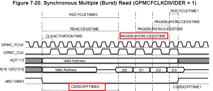
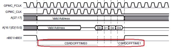
1.We couldn't understand why Synchronous Multiple (Burst) Read (Figure 7-20) has
CSRDOFFTIME is divided into two (CSRDOFFTIME0 and CSRDOFFTIME1)
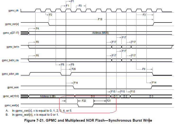
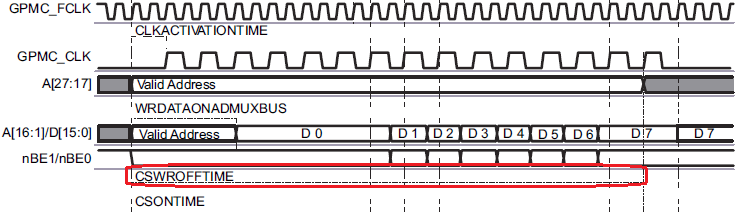
whereas Synchronous Multiple (Burst) write(Figure 7-22) has one CSWROFFTIME?
Synchronous Multiple (Burst) Read:
Synchronous Multiple (Burst) write:
2.As per the the Datasheet "Table 7-22" the chip select pulse duration tw(csnV) is
calculated with the below equation.
A = (CSRdOffTime – CSOnTime + (n – 1) × PageBurstAccessTime) × (TimeParaGranularity + 1) × GPMC_FCLK
With the above equation the burst time is calculated with the difference of
CSOffTime and CSOnTime and we believe it will be a big value.
In case of actual design do we need to follow both datasheet calculation and
the TRM manual(Figure 7-20/Figure 7-22) as well?
Best Regards
Kummi