This thread has been locked.

If you have a related question, please click the "Ask a related question" button in the top right corner. The newly created question will be automatically linked to this question.

AM5728: DDR3 compliance test fails

Part Number: AM5728
Other Parts Discussed in Thread: AM5718

Hi,

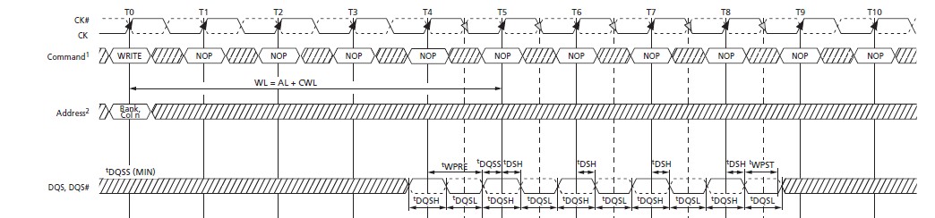
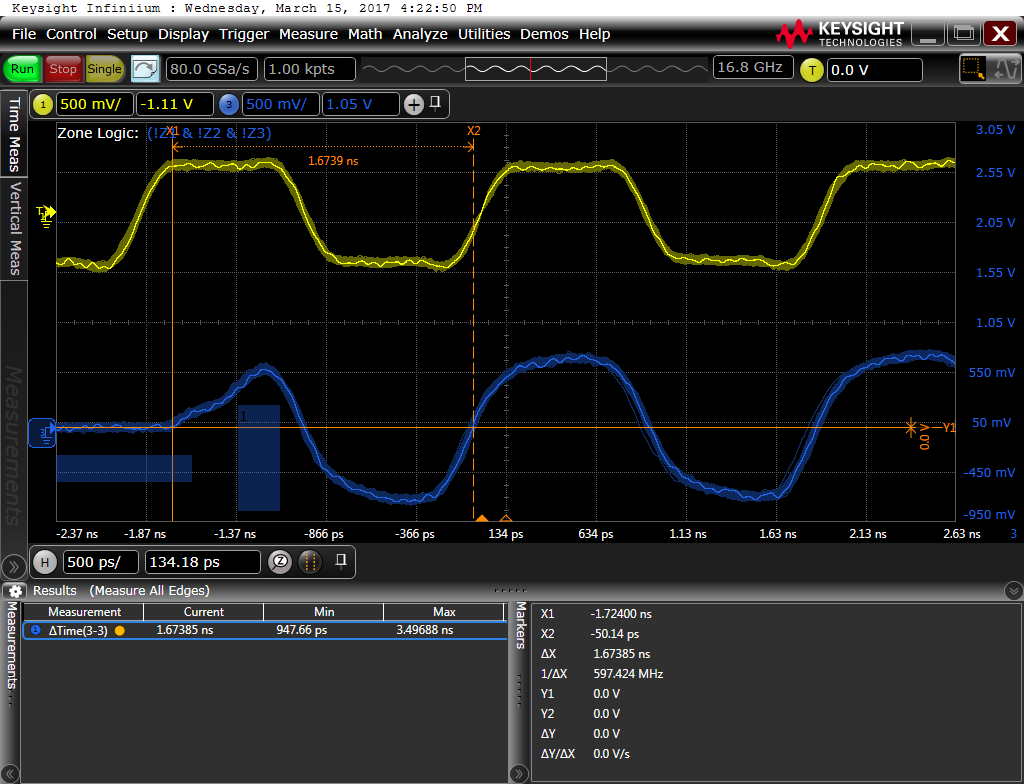
Our customer fails in a timing of tWPRE of DDR3 compliance test of AM572x.

A start of DQS of the tWPRE section is late, and it does not satisfy min of tWPRE(0.9*tck).
Please confirm the following wave pattern.

Yellow: CK signal
Blue: DQS signal

The following countermeasures were taken, but in both cases the timing of tWPRE did not satisfy spec.

1.A change of DDR_TERM bit
2.A change of SDRAM_DRIVE bit
3.The change of PHY_INVERT_CLKOUT bit and the PHY_REG_CTRL_SLAVE_RATIO0 bit
4.The change of the DDR3CH2_PART6_I[7:5] bit of the CTRL_CORE_CONTROL_DDRCACH2_0 register
5.The change of the DDRCH2_PART4B_I[7:5] bit of the CTRL_CORE_CONTROL_DDRCH2_1 register
6.The change of the DDRCH2_PART4B_I[7:5] bit of the CTRL_CORE_CONTROL_DDRCH2_1 register
7.I change terminal resistance of the CK into 51 Ω from 39 Ω.

There are two questions.
1.How can we do to increase the tWPRE section of DQS or to speed up the rise time of tWPRE?
Please tell me how to do it.

2.Does the problem that tWPRE timing does not meet spec in other users using AM572x not occur?

Best Regards,
Shigehiro Tsuda

  • Hi,

    Is this a custom board? Did you follow this guide: www.ti.com/.../sprac36.pdf
  • Hi Biser,

    Thank you for quick reply.
    Yes,this is a custom board.

    They follow that document, but only the timing of tWPRE is short.
    tWPRE is not described in that document.
    Data can be read and written normally, and the waveform of DQS other than tWPRE is also satisfied.
    It only has a condition that tWPRE timing of the compliance test of DDR3 is failed.

    Is there any information?

    Best Regards,
    Shigehiro Tsuda
  • I will ask the DDR experts to comment. They will respond here.
  • Hi Biser,

    Thank you for quick reply.
    Is there any update information from the DDR experts?

    Best Regards,
    Shigehiro Tsuda
  • I will check what happened and escalate.
  • Can you share more details of the DRAM part, schematics and the DDR configuration obtained through the EMIF tool to debug this further? Also, if you have the DDR compliance report, please do fwd. us. If these cannot be shared on the forum, please let us know so we can reach out to you.

    Regards, Siva

  • We received the information you shared with us. I reviewed the DDR configuration and it does not reflect the correct settings. I have found several errors in the ddr_setting file you provided. If you still believe this is correct, please share the corresponding spread sheet that was used to arrive at the values.

    If the EMIF tool was not used, can you setup the EMIF tool and make sure you enable HW leveling? After you have HW leveling done, perform the DDR compliance test. Please let us know what you find after you re-do the tests.

    Regards, Siva
  • Hi Siva,

    Thank you for quick reply.

    Thank you for reviewing customer's DDR3 configuration results.
    It seems our customers did not use the EMIF tool.
    Use the EMIF tool to update the value to u - boot, perform hardware leveling, and have the DDR 3 compliance test run.

    Best Regards,
    Shigehiro Tsuda
  • Hi Siva,

    Thank you for your kind support.

    Our customers confirmed with the value calculated by AM57xx EMIF tools, but the tWPRE timing was not different from the previous measurement result.

    They have the following questions.

    From the IBIS model of AM5718, the internal circuit of the DQS buffer is as follows
    There seems to be an ENABLE signal outputting the internal DQS to the outside.

    Adjust the timing to put this ENABLE signal and as shown below DQS
    Will not the tWPRE increase as early as the beginning of the rise?
    Please let me know if there is a register to set the timing to insert this ENABLE signal.

    Best Regards,
    Shigehiro Tsuda

  • Tsuda-san

    I'm checking this. Are the results exactly same as the report before?

    Regards, Siva

  • Tsuda-san

    Please see the attached PDF. I suspect if you are using the right DQS edge for calculating the tWPRE? Could you zoom out and check the burst and see if you are using the right DQS edge. If not, please adjust the measurement as I indicated in the PDF and see if it meets the spec.

    Regards, Siva

    tWRPRE Update .pdf

  • Hi Siva,

    Thank you for quick reply.
    I referred to the attached documentation of you. As you said, the second waveform may be tWPRE, so we will enlarge the range and measure the data as well.

    Best Regards,
    Shigehiro Tsuda
  • Hi Siva,

    Thank you for various support.

    According to your answer, DQ1 was added and measured, it turned out that the timing confirmed as tWPRE was different.
    For details, please refer to the following.
    We have the following two questions.
    ① Which of red and blue will be the timing of tWPRE?
    ② For tWPRE, is it the specification of AM57xx that DQS starts high / low switching operation before the original write preamble period?

    Measurement result:
    Waveform colors are as follows.
    Yellow: CK
    Blue: DQS
    Green: DQ 1
    When writing, write High all data

    Best Regards,
    Shigehiro Tsuda

  • Tsuda-san

    Please see the snapshots below. Basically, the tWPRE should be measured - Basically, one clock cycle before the actual WRITE DQ input to the DRAM is when you should be measuring the tWPRE. From your scope capture, I'm unable to figure out when the actual WRITE command is sent to the DRAM to determine the right clock edge for tWPRE measurement. Please refer to your memory data sheet which should provide information about how to measure tWPRE for different scenarios.

  • Tsuda-san

    Please see the snapshot below. Basically, one clock cycle before the actual WRITE DQ input to the DRAM is when you should be measuring the tWPRE. From your scope capture, I'm unable to figure out when the actual WRITE command is sent to the DRAM to determine the right clock edge for tWPRE measurement. Please refer to your memory data sheet which should provide information about how to measure tWPRE for different scenarios.

    Regards, Siva

  • Hi Siva,

    Thank you for quick reply.

    The failure problem of this time is caused by a change in the DQS signal before the correct tWPRE and the measuring instrument regarded the change as tWPRE.
    Could you tell me the answer for the following?

    For tWPRE, is it the specification of AM57xx that DQS starts high / low switching operation before the original write preamble period?

    Best Regards,
    Shigehiro Tsuda

  • Hi Siva,

    Thank you for various support.

    Our customers also added the WE signal and measured it.
    From the results, the initial waveform change seems to be tWPRE.

    From WL=AL+CWL=0+6=6, 18.8nsx6=11.28ns from issuance of write command to output of write data.
    (Operating frequency is 532 MHz)
    On the waveform this time roughly matched the time from WE=L to the leading rise waveform of DQS.

    It seems that timing of min 0.9 * tck or more of DDR3L tWPRE is not observed. For details, please check the following.
    Is it possible to control the timing of this tWPRE?
    Can it be adjusted with PHY registers?
    It is said that our customer want measured waveform data.
    is it possible to respond?

    Best Regards,
    Shigehiro Tsuda

  • Hi Siva,

    Is there any update information?

    Best Regards,
    Shigehiro Tsuda
  • Sorry for the delay...Siva is working on it...

  • Tsuda-san

    shigehiro tsuda said:

    Our customers also added the WE signal and measured it.
    From the results, the initial waveform change seems to be tWPRE.

    Thanks for confirming this. So, it looks like the initial measurement for tWPRE is accurate and uses the right DQS edge.

    shigehiro tsuda said:

    From WL=AL+CWL=0+6=6, 18.8nsx6=11.28ns from issuance of write command to output of write data.
    (Operating frequency is 532 MHz)
    On the waveform this time roughly matched the time from WE=L to the leading rise waveform of DQS.

    OK. I agree.

    shigehiro tsuda said:

    It seems that timing of min 0.9 * tck or more of DDR3L tWPRE is not observed. For details, please check the following.
    Is it possible to control the timing of this tWPRE?
    Can it be adjusted with PHY registers?
    It is said that our customer want measured waveform data.
    is it possible to respond?

    Are you indicating the min. tWPRE is not satisfied based on the original measurements after confirming the correct DQS edge? I also reviewed the report that you sent and have the following suggestions.

    I don't think there is any timing parameter that can be adjusted with PHY registers to adjust tWPRE timing. I did not understand what the customer wants. Which measured waveform data is the customer expecting? Could you please clarify.

    Can you check the following?

    - Adjust Data drive strength and SDRAM ODT settings to see if there is any difference in the results?

    - Are you using Dynamic ODT of the SDRAM? If so, can you disable Dynamic ODT and see any difference?

    - Is the layout meeting all the data sheet requirements?

    Regards, Siva

  • Tsuda-san

    shigehiro tsuda said:

    Our customers also added the WE signal and measured it.
    From the results, the initial waveform change seems to be tWPRE.

    Thanks for confirming this. So, it looks like the initial measurement for tWPRE is accurate and uses the right DQS edge.

    shigehiro tsuda said:

    From WL=AL+CWL=0+6=6, 18.8nsx6=11.28ns from issuance of write command to output of write data.
    (Operating frequency is 532 MHz)
    On the waveform this time roughly matched the time from WE=L to the leading rise waveform of DQS.

    OK. I agree.

    shigehiro tsuda said:

    It seems that timing of min 0.9 * tck or more of DDR3L tWPRE is not observed. For details, please check the following.
    Is it possible to control the timing of this tWPRE?
    Can it be adjusted with PHY registers?
    It is said that our customer want measured waveform data.
    is it possible to respond?

    Are you indicating the min. tWPRE is not satisfied based on the original measurements after confirming the correct DQS edge? I also reviewed the report that you sent and have the following suggestions.

    - Are you using proper FET probes to get all the measurements? I'm also wondering since the difference is in the order of 10's of ps, if this is caused due to any measurement errors

    - Is this particular failure causing any issues in the actual DRAM behavior?

    - did you notice this only at 532MHz DDR clock speed or is it occurring even at lower speeds? If you have not tried a lower speed, can you please check if you find a similar behavior?

    I don't think there is any timing parameter that can be adjusted with PHY registers to adjust tWPRE timing. I did not understand what the customer wants. Which measured waveform data is the customer expecting? Could you please clarify.

    Can you also check the following?

    - Adjust Data drive strength and SDRAM ODT settings to see if there is any difference in the results?

    - Are you using Dynamic ODT of the SDRAM? If so, can you disable Dynamic ODT and see any difference?

    - Is the layout meeting all the data sheet requirements?

    Regards, Siva

  • Hi Siva,

    Thank you for quick reply and some supports.

    [your question]
    Are you using proper FET probes to get all the measurements? I'm also wondering since the difference is in the order of 10's of ps, if this is caused due to any measurement errors

    [answer]
    Yes,they use proper FET probes and they are confirming it to the measuring equipment company while confirming it is correct as a measurement.

    [your question]
    Is this particular failure causing any issues in the actual DRAM behavior?

    [answer]
    Yes,the data in DDR3 can be read and written normally.

    [your question]
    did you notice this only at 532MHz DDR clock speed or is it occurring even at lower speeds? If you have not tried a lower speed, can you please check if you find a similar behavior?

    [answer]
    I confirm to them how they will look if they slow down the clock's operating frequency of DDR3.
    Please wait.

    [your question]
    Adjust Data drive strength and SDRAM ODT settings to see if there is any difference in the results?

    [answer]
    I confirmed the above, but there was a response from the customer that there was no change in the waveform of tWPRE.

    [your question]
    Are you using Dynamic ODT of the SDRAM? If so, can you disable Dynamic ODT and see any difference?

    [answer]
    Since it is written that TRM of AM 572x does not support Dynamic ODT, it is operating with disable setting.
    Is it usable?

    [your question]
    Is the layout meeting all the data sheet requirements?

    [answer]
    We are listening from our customers that they are designing to keep the DDR3 layout rules of the data sheet.

    It is impossible to judge whether the controller outputs the timing waveform of this tWPRE or whether there is an external factor.
    Our customers want the result of measuring the waveform of tWPRE.
    Is it possible to respond?

    Best Regards,
    Shigehiro Tsuda
  • Tsuda-san

    Thanks for your responses. Please provide more information as you hear from the customer on the items you listed above.

    >>
    It is impossible to judge whether the controller outputs the timing waveform of this tWPRE or whether there is an external factor.
    Our customers want the result of measuring the waveform of tWPRE.
    Is it possible to respond?
    >>

    Can you help what exactly is the customer looking for here? I'm not sure what could be causing this failure. If you are looking for impact of not meeting the tWPRE as measured in your tests, I suggest you contact the memory vendor since this is specific to the DRAM timings and not the SoC.

    Regards, Siva
  • Tsuda-san

    Is there any update on this thread? Let me know if you need any other information here

    Regards, Siva
  • Hi Siva,

    Thank you for your support.
    Sorry for my late reply.

    They had the following waveform checked, but in all environments the interval of tWPRE was less than 0.9 * tCK.
    ① different boards
    ② Change of measuring equipment

    Currently, we have tried by changing the following setting values.
    • Output impedance controls - I [2: 0]
    • Slew rate controls - SR [2: 0]
    • Weak driver controls - WD [1: 0]
    18.4.6.10 Software Controls for the DDR2/DDR3 I/O Cells
    • ODT controls

    Does the AM572x support Dynamic ODT?

    Please let me know if there is such information that the tWPRE timing becomes longer or the timing of rise becomes faster.

    Best Regards,
    Shigehiro Tsuda