This thread has been locked.

If you have a related question, please click the "Ask a related question" button in the top right corner. The newly created question will be automatically linked to this question.

TMS320C6670: PCIe outbound payload size with EDMA

Part Number: TMS320C6670

Hello!

Some time ago there was similar thread about PCIe outbound size in C6678. Though the thread was marked as resolved, I don't see how exactly that helped. Now its my turn to ask exactly same.

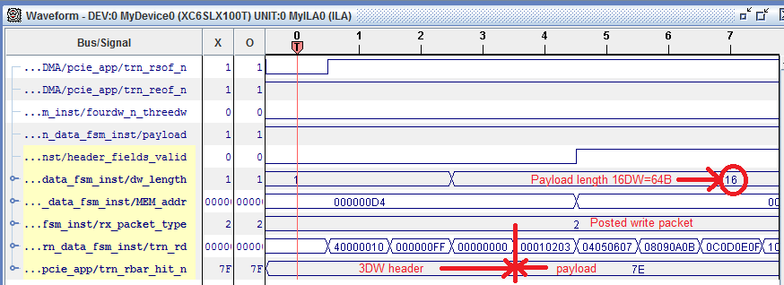
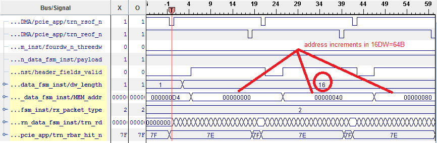
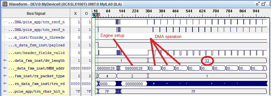
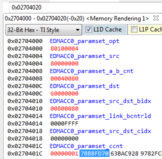
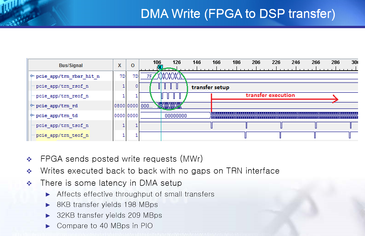
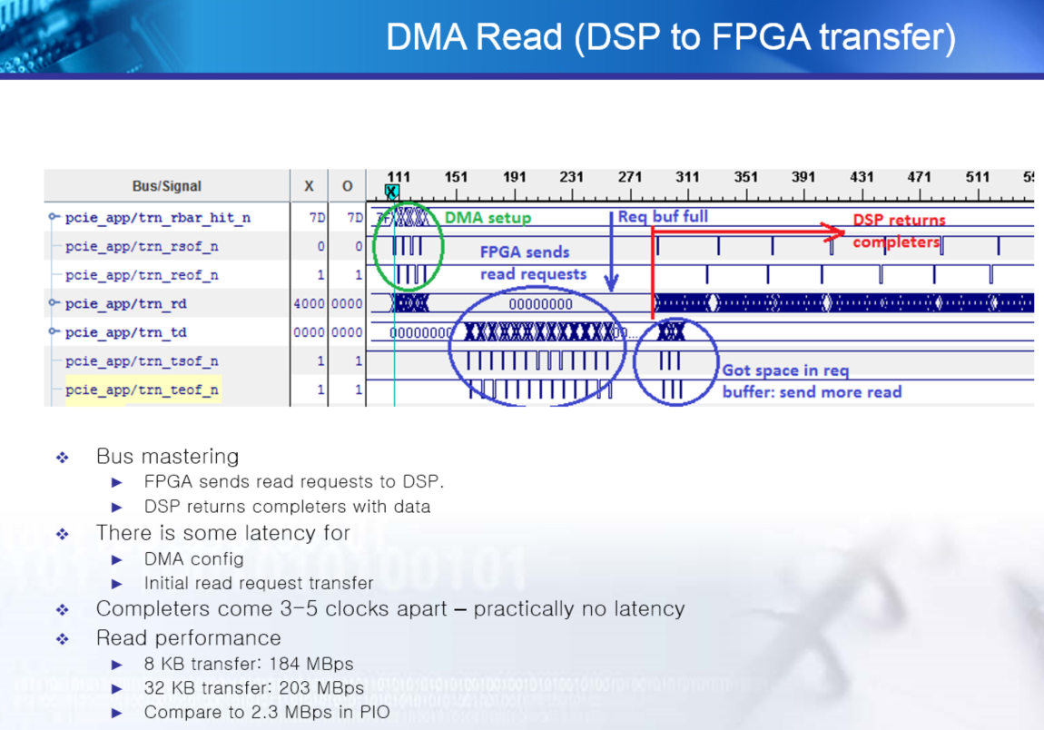
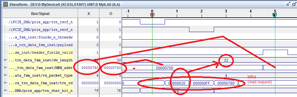
I have C6670. I am setting EDMA transfer through EDMACC0, whose both transfer controllers have DBS of 128B. I am setting transfer size of 2K. I am monitoring PCIe transaction interface on EP, which is FPGA. I see TLP come with payload size of 16 DWORDs, that is 64B. Also I see 32 transfers, thus 2048B/32=64B per transfer. Moreover, in TLP header I see destination address as 0x0000, 0x0040, 0x0080, they increments in multiples of 64B.

On the other hand, I am sure my FPGA advertises DEV_CAP_MAX_PAYLOAD_SUPPORTED parameter as 128B.

Thus once again I'd like to ask, how do I enforce 128B outbound transfer using EDMA over PCIe.

Thanks in advance.

  • Hi,

    I've notified the factory team. Their feedback will be posted here.

    Best Regards,
    Yordan
  • Hi,

    Your observation is that the OB payload size is actually 64 bytes. I don't have the scope to check the TLP payload. In the past we have test of the PCIE throughput with different EDMA transfer controllers either with 64 bytes or 128 bytes DBS and the number we got matchs the theorical throughput, so we think the OB payload size is correct. The test was done between TI EVMs, we didn't do anything special in PCIE registers to force 128 bytes. The OB limitation comes from EDMA DBS size. On the IB direction, the PCIE suppports 256 bytes payload.

    C6670 EDMA CC0 has both controllers of 128 bytes DBS. What is your ACNT and BCNT setting in this case and you used A-SYNC or A-B Sync?

    What is the TI 6670 side DEV_CAP setting, 0x2180_1074, BIT 2-0? And DEV_STAT_CTRL, 0X2180_1078, bit 7-5? 0 means 128 bytes, 1 means 256 bytes.

    Regards, Eric
  • Hi Eric,

    Thank you for your care. Upon configuration my settings are:

    DEVICE_CAP 0x21801074 00008001 ==> 1 is for 256B

    DEV_STAT_CTRL 0x21801078 0000281F ==> 1 is for 256B

    I wonder a little why that might have any influence, as minimum size allowed to advertise by spec is 128B.

    I had experience with DMA engine on EP side, in FPGA. I was able to issue 128B writes and read requests from FPGA to DSP and they worked as expected. Particularly, in Gen. x1 configuration I could have over 200MBps on large transfers.

    Here is my config for the trasfer

            dma->rght.prm.cfg.option = CSL_EDMA3_OPT_MAKE
            (
                CSL_EDMA3_ITCCH_DIS,        // itcchEn,
                CSL_EDMA3_TCCH_DIS,         // tcchEn,
                CSL_EDMA3_ITCINT_DIS,       // itcintEn,
                CSL_EDMA3_TCINT_EN,         // tcintEn,
                FPGA_EDMA_TX1_R,            // tcc,
                CSL_EDMA3_TCC_NORMAL,       // tccMode,
                CSL_EDMA3_FIFOWIDTH_NONE,   // fwid,
                CSL_EDMA3_STATIC_DIS,       // stat,
                CSL_EDMA3_SYNC_A,           // syncDim,
                CSL_EDMA3_ADDRMODE_INCR,    // dam,
                CSL_EDMA3_ADDRMODE_INCR     // sam
            );
            dma->rght.prm.cfg.srcAddr     = (Uint32) pcie_l2_buf.buf;//pcie_buf;
            dma->rght.prm.cfg.aCntbCnt    = CSL_EDMA3_CNT_MAKE( 2*1024, 1 );
            dma->rght.prm.cfg.dstAddr     = (Uint32) 0x60000000;
            dma->rght.prm.cfg.srcDstBidx  = CSL_EDMA3_BIDX_MAKE( 1, 1 );
            dma->rght.prm.cfg.linkBcntrld = CSL_EDMA3_LINKBCNTRLD_MAKE( CSL_EDMA3_LINK_DEFAULT, 0 );
            dma->rght.prm.cfg.srcDstCidx  = CSL_EDMA3_CIDX_MAKE( 0, 1 );
            dma->rght.prm.cfg.cCnt        = 1;
    

    I am willing to investigate this issue. Thank you for assistance.

  • Hi,

    Those two registers I just want to double check what were programmed as I don't know what SW you used. I want to make if it is reasonable value for maxmium payload size.

    I looked your DMA configuration, it looks right that CSL_EDMA3_CNT_MAKE( 2*1024, 1 ); will put 2048 into ACNT and 1 into BCNT. And the EDMA TC will split 2048 bytes with DBS.

    Something you can try:
    1) change CSL_EDMA3_SYNC_A to CSL_EDMA3_SYNC_AB
    2) transfer a bigger chunk, let say 128KB with dma->rght.prm.cfg.aCntbCnt = CSL_EDMA3_CNT_MAKE( 128, 1024 );

    Also, can you double check if this is really EDMA CC0?

    Regards, Eric
  • Hi!

    Thank you again for the attention to my difficulty. I'll paste relevant code fragments, because its seems that there is more than one issue I have.

    Here is common init code, opening edma instance 0

    #define FPGA_EDMA_CC_INST       CSL_EDMA3CC_0
    
    edma_str *edma_init(void)
    {
        CSL_Status status;
    
        edma_str *dma = (edma_str *) malloc(sizeof(edma_str));
        if ( NULL == dma ) return NULL;
        
        // Module Initialization
        CSL_edma3Init( NULL );    // Always returns CSL_SOK
    
        // Module Level Open
        // Only EDMACC0 can have Data Burst Size (DBS) of 128B, which we want to
        // have with PCIe transfers.
        dma->hModule = CSL_edma3Open( &dma->moduleObj, FPGA_EDMA_CC_INST, NULL, &status );
        if ( CSL_SOK != status ) return edma_close(dma);
    
        if ( NULL == ( dma->fpga = fpga_dma_init(dma->hModule) ) ) return edma_close(dma);
    
        return dma;
    }

    Next I have specific channel setup:

    fpga_dma_str *fpga_dma_init( CSL_Edma3Handle hModule )
    {
        CSL_Status                  status;
        CSL_Edma3ChannelAttr        chAttr;
    
        fpga_dma_str *dma = (fpga_dma_str *) malloc(sizeof(fpga_dma_str));
        if (NULL == dma) return NULL;
    
        //
        /* Open EDMA channels */
        chAttr.regionNum = CSL_EDMA3_REGION_GLOBAL;
        chAttr.chaNum    = FPGA_EDMA_TX1_R;
        dma->tx1.rght.cha.hdl = CSL_edma3ChannelOpen( &dma->tx1.rght.cha.obj, FPGA_EDMA_CC_INST, &chAttr, &status );
        if ( (NULL == dma->tx1.rght.cha.hdl) || (CSL_SOK != status) )
            return fpga_dma_close( dma );
    
        if ( CSL_SOK != CSL_edma3HwChannelSetupQue(dma->tx1.rght.cha.hdl, FPGA_EDMA_QUE) )
            return fpga_dma_close( dma );
    
        /* Map the DMA Channel to PARAM Block. */
        CSL_edma3MapDMAChannelToParamBlock( hModule, FPGA_EDMA_TX1_R, 8 * FPGA_EDMA_TX1_R );
    
        dma->tx1.rght.prm.hdl = CSL_edma3GetParamHandle( dma->tx1.rght.cha.hdl, 8 * FPGA_EDMA_TX1_R, &status );
        if ( (NULL == dma->tx1.rght.prm.hdl) || (CSL_SOK != status) )
            return fpga_dma_close( dma );
    
        return dma;
    }

    Here

    #define FPGA_EDMA_TX1_R     6

    Then before every transfer I apply configuration:

    void fpga_tx_edma_mk_cfg
    (
        u_int8      *src,   /* Src address for TX.   Channel ignored if NULL    */
        u_int8      *dst,   /* Dst address for TX.   Channel ignored if NULL    */
        tx_dma_str  *dma    /* EDMA resources for TX transfer                   */
    )
    {       
    
        if ( (NULL != src) && (NULL != dst) )
        {
            /* Setup the parameter entry parameters */
            dma->rght.prm.cfg.option = CSL_EDMA3_OPT_MAKE
            (
                CSL_EDMA3_ITCCH_DIS,        // itcchEn,
                CSL_EDMA3_TCCH_DIS,         // tcchEn,
                CSL_EDMA3_ITCINT_DIS,       // itcintEn,
                CSL_EDMA3_TCINT_EN,         // tcintEn,
                FPGA_EDMA_TX1_R,            // tcc,
                CSL_EDMA3_TCC_NORMAL,       // tccMode,
                CSL_EDMA3_FIFOWIDTH_NONE,   // fwid,
                CSL_EDMA3_STATIC_DIS,       // stat,
                CSL_EDMA3_SYNC_AB,           // syncDim,
                CSL_EDMA3_ADDRMODE_INCR,    // dam,
                CSL_EDMA3_ADDRMODE_INCR     // sam
            );
            dma->rght.prm.cfg.srcAddr     = (Uint32) src;//pcie_buf;
            dma->rght.prm.cfg.aCntbCnt    = CSL_EDMA3_CNT_MAKE( 256, 2 );
            dma->rght.prm.cfg.dstAddr     = (Uint32) dst;
            dma->rght.prm.cfg.srcDstBidx  = CSL_EDMA3_BIDX_MAKE( 256, 256 );
            dma->rght.prm.cfg.linkBcntrld = CSL_EDMA3_LINKBCNTRLD_MAKE( CSL_EDMA3_LINK_DEFAULT, 0 );
            dma->rght.prm.cfg.srcDstCidx  = CSL_EDMA3_CIDX_MAKE( 0, 0 );
            dma->rght.prm.cfg.cCnt        = 1;
    
           /* Place setup */
           CSL_edma3ParamSetup(dma->rght.prm.hdl, &dma->rght.prm.cfg);
        }
    }
    

    Finally I trigger the transfer manually as

    void fpga_tx_edma_submit(tx_dma_str *dma)
    {
        if ( NULL != dma )
        {
            if ( NULL != dma->rght.cha.hdl )
            {
                edma_start = TSCL;
                CSL_edma3ParamSetup(dma->rght.prm.hdl, &dma->rght.prm.cfg);
                CSL_edma3HwChannelControl(dma->rght.cha.hdl, CSL_EDMA3_CMD_CHANNEL_SET, NULL );
            }
        }
    }
    

    So throughout of this code I see only EDMACC0 was mentioned. Also, as indirect indication that right controller was used, I could see completion interrupt happening with the following config:

    EventCombiner.eventGroupHwiNum[0] = 7;
    EventCombiner.eventGroupHwiNum[1] = 8;
    EventCombiner.eventGroupHwiNum[2] = 9;
    EventCombiner.eventGroupHwiNum[3] = 10;
    
    CpIntc.sysInts[36].fxn      = '&edma_isr';
    CpIntc.sysInts[36].arg      = 36;
    CpIntc.sysInts[36].hostInt  = 2;
    CpIntc.sysInts[36].enable   = true;
    
    var eventId = CpIntc.getEventIdMeta(2);
    params               = new Hwi.Params;
    params.arg           = 2;
    params.instance.name = 'edma';
    params.eventId       = eventId;
    params.enableInt     = 1;
    Program.global.hwi11 = Hwi.create(6, CpIntc.dispatch, params);
    

    I believe I've set completion interrupt with System Event 36 which is EDMACC0 completion in global region. So far should be OK.

    What is bad, is that data I receive are wrong. Actually, in FPGA all payload codes as zero, I only see 3 DWORDS of TLP header, they look fine, but whole payload is just zero. To make sure, I have created static array filled with byte counts and flushed the cache:

    u_int8 edma_buf[128*64];
    
            int i;
    
            for ( i = 0; i < 1024; i++ ) edma_buf[i] = i;
            Cache_wbInv( (xdc_Ptr)(edma_buf), sizeof(edma_buf), Cache_Type_L2, TRUE );
            fpga_tx_edma_mk_cfg( edma_buf, (u_int8*)0x60000000, FFTN_2048, &lte->dma->fpga->tx1 );
            edma_intr_enable( lte->dma->hModule );
            fpga_tx_edma_submit( &lte->dma->fpga->tx1 );

    As to your suggestion about different transfers configurations I should report the following:

    1) If I make any bigger block with A-sync, I see only dimension A transferred in units of 64B, e.g. for the following config

    dma->rght.prm.cfg.option = CSL_EDMA3_OPT_MAKE
            (
                CSL_EDMA3_ITCCH_DIS,        // itcchEn,
                CSL_EDMA3_TCCH_DIS,         // tcchEn,
                CSL_EDMA3_ITCINT_DIS,       // itcintEn,
                CSL_EDMA3_TCINT_EN,         // tcintEn,
                FPGA_EDMA_TX1_R,            // tcc,
                CSL_EDMA3_TCC_NORMAL,       // tccMode,
                CSL_EDMA3_FIFOWIDTH_NONE,   // fwid,
                CSL_EDMA3_STATIC_DIS,       // stat,
                CSL_EDMA3_SYNC_A,           // syncDim,
                CSL_EDMA3_ADDRMODE_INCR,    // dam,
                CSL_EDMA3_ADDRMODE_INCR     // sam
            );
            dma->rght.prm.cfg.srcAddr     = (Uint32) src;//pcie_buf;
            dma->rght.prm.cfg.aCntbCnt    = CSL_EDMA3_CNT_MAKE( 256, 16 );
            dma->rght.prm.cfg.dstAddr     = (Uint32) dst;
            dma->rght.prm.cfg.srcDstBidx  = CSL_EDMA3_BIDX_MAKE( 256, 256 );
            dma->rght.prm.cfg.linkBcntrld = CSL_EDMA3_LINKBCNTRLD_MAKE( CSL_EDMA3_LINK_DEFAULT, 0 );
            dma->rght.prm.cfg.srcDstCidx  = CSL_EDMA3_CIDX_MAKE( 0, 0 );
            dma->rght.prm.cfg.cCnt        = 1;

    I see 4 transfers of 64B, and yeah, with zero payload.

    If I make this transfer with AB-sync, then whole block is transferred in chunks of 64B.

    Please assist in debugging.

    Thanks in advance.

  • Hi,

    It looks that you have two issues: 1) 64byte transfer regardless of DBS 2) TLP payload is zero

    1) do you have a stead PCIE link between C6657 and FPGA?

    2) The code looks right to use EDMA CC0 and channel 6. Before you manually trigger the transfer, are you able to download the paramSet starting from register 0x27040A0 to 0x27040C0 (this is for CC0, channel 6, each channel uses 0x20). You can decode if they look right or not. Then look at the SRC address, is it your EDMA data source buffer. What you see the content in CCS memory window with cache checked and unchekced for this source buffer, zero or your pattern? What is your EDMA DST? Is it 0x60000000?

    Then after the transfer, what do you see in 0x60000000? zero or your data pattern? If zero, can you manually write 0x60000000 to something in CCS memory window? or can you use code like *(unsigned int*)0x60000000 = pattern writing into it? I want to understand if 0x60000000 region is writable or not?

    Regards, Eric
  • Hi Eric,

    For the second issue with zeroed payload I guess I know the reason: I forgotten to convert buffer address, which I am sure was core local, to global address when telling EDMA source address. Though confident about that, will confirm on hardware and report.

    I don't know, whether above failure has any relation to issue #1 with 64B fragmentation. Will fix and check again.

    As to PCIe link to FPGA, it is proven operational design. As present we have DMA engine in FPGA, it performs bulk reads and writes together with PIO transfers. With that machine we were able to exchange TLPs with 128B payload in both directions with throughput over 200MBps with larger blocks on x1 Gen.1 link. Sure, there is translation code for PCIe data window, but that was verified for years.

    Thank you for the hint to peep and decode paramset memory location. Will do that and report.

    It looks like we stay on the opposite sides of the Globe, I am already out of the office for weekend, but will check and report on Monday.

    Thank you very much for guiding me, that's real value for me.

  • Hello Eric,

    I have just confirmed my suspicion: zero payload was due to my failure to submit buffer's global address to EDMA engine. See the capture at FPGA transaction  interface

    After 3 DWORDS of TLP Header there is payload as I expected it to see. Mea culpa.

    However, the issue with TLP payload size still there. On the picture above one ma see 'dw_length' signal showing 16DW=64B. In some larger scale:

    Note, MEM_addr signal increments by 0x40, which again is 64B.

    Just to make sure, I have triggered DSP-to-FPGA transfer using DMA engine in FPGA:

    Note, that after transfer setup, data coming in packets with 32DW=128B payload. Packet type is different, because FPGA was requesting reads, and DSP responds with Completer TLPs. Important conclusion from this experiment is that PCIe subsystem is capable to form and transfer 128B payload. However, that does not happen, when PCIe transfer was requested by EDMA.

    As to transfer speed, I made rough experiment and saw transfer rate of about 180MBps comparing to 200+MBps with FPGA's engine.

    We may estimate link utilization ratio as (64B payload) / (64B payload + 12B header) = 84% versus (128B payload) / (128B payload + 12B header) = 91%. Not critical, but visible.

    I see the handle to paramset in my case is 0x02704600. At that address I see reasonable parameters landed. Perhaps, that needs more attention, but in any case, the true issue is payload size in EDMA initiated transfers.

    Please assist debugging that.

    Thanks in advance.

    Victor

  • Hi again,

    When selecting PaRAM entry, I place

    CSL_edma3MapDMAChannelToParamBlock( hModule, FPGA_EDMA_TX1_R, 8 * FPGA_EDMA_TX1_R );

    That is entry #48, thus 48*0x20=0x600, and handle I've got 0x02704600 is correct. I made sure all configuration values from my config structure land to PaRAM location exactly the same. I am afraid, I am missing something important, that A-sync transfers don't work as I expect, but at least AB-sync transfers run well, and with them I definitely see TLP payload of 64B, which is less than expected DBS fragmentation. Let us concentrate on this issue.

    Victor

  • Hello!

    As I suspected, misbehaviour of A-sync transfers was my fault too. A-sync transfer implies intermediate chaining enabled. When I fixed that, both A-sync and AB-sync transfers move whole expected block.

    However, in both cases I see that TLP payload size is 64B. I wish to dig it. Will run your reference examples on my h/w if needed.

    Thanks.

    Victor

  • Hi,

    From Table 7-33, EDMACC0 only has 16 channles. However, you used channel 48? Can you just use the channel 0? Checking the paramSet at 0x2704000 and checking if the TLP payload is 64 or 128 bytes?

    Regards, Eric
  • Hello Eric,

    Thank you keep helping me. I believe I was using legal combination:

    #define FPGA_EDMA_TX1_R     6
    
    chAttr.chaNum    = FPGA_EDMA_TX1_R;
    ...
    CSL_edma3ChannelOpen( &dma->tx1.rght.cha.obj, FPGA_EDMA_CC_INST, &chAttr, &status );
    ...
    CSL_edma3MapDMAChannelToParamBlock( hModule, FPGA_EDMA_TX1_R, 8 * FPGA_EDMA_TX1_R );
    ...
    CSL_edma3GetParamHandle( dma->tx1.rght.cha.hdl, 8 * FPGA_EDMA_TX1_R, &status );
    

    So the channel was #6, but PaRAM set #48. EDMA3CC0 should have 16 channels, but 128 PaRAM entries.

    Nevertheless, I have tried with channel #0, PaRAM set #0. Parameter landed to memory were:

    In my code I had:

    dma->rght.prm.cfg.option = CSL_EDMA3_OPT_MAKE
            (
                CSL_EDMA3_ITCCH_DIS,        // itcchEn,
                CSL_EDMA3_TCCH_DIS,         // tcchEn,
                CSL_EDMA3_ITCINT_DIS,       // itcintEn,
                CSL_EDMA3_TCINT_EN,         // tcintEn,
                FPGA_EDMA_TX1_R,            // tcc,
                CSL_EDMA3_TCC_NORMAL,       // tccMode,
                CSL_EDMA3_FIFOWIDTH_NONE,   // fwid,
                CSL_EDMA3_STATIC_DIS,       // stat,
                CSL_EDMA3_SYNC_AB,           // syncDim,
                CSL_EDMA3_ADDRMODE_INCR,    // dam,
                CSL_EDMA3_ADDRMODE_INCR     // sam
            );
            dma->rght.prm.cfg.srcAddr     = (Uint32) src;//pcie_buf;
            dma->rght.prm.cfg.aCntbCnt    = CSL_EDMA3_CNT_MAKE( 128, 4 );
            dma->rght.prm.cfg.dstAddr     = (Uint32) dst;
            dma->rght.prm.cfg.srcDstBidx  = CSL_EDMA3_BIDX_MAKE( 128, 128 );
            dma->rght.prm.cfg.linkBcntrld = CSL_EDMA3_LINKBCNTRLD_MAKE( CSL_EDMA3_LINK_DEFAULT, 0 );
            dma->rght.prm.cfg.srcDstCidx  = CSL_EDMA3_CIDX_MAKE( 0, 0 );
            dma->rght.prm.cfg.cCnt        = 1;

    For OPT field we see

    • PRIV=1 - have no idea;
    • TCINTEN=1 - just right;
    • SYNCDIM=1 - matches CSL_EDMA3_SYNC_AB.

    Src, Dst addresses as well as counts seems right too. However, even in this case still I see 64B payload size. This behaviour is observed as for AB-sync transfers, so for A-sync transfers. I have tried blocks as large as 128*1024.

    Let's see, what else to check. Thanks in advance.

    Victor

  • Hi,

    PRIV = 1 is Supervisor level privilege, this is expected. I didn't see anything wrong in the code, I don't have scope setup to capture PCIE TLP to determine the payload size. So we normally run the PCIE throughput test with different CC/TC combination, to show the DBS in the TC as expected by seeing the difference in throughput.

    In the www.ti.com/.../sprabk8.pdf, 2.4 Measured Throughput, you may take a look. C6678 and C6670 should be the same. In example 5, there is EDMA configuration example code. You may double check.

    Regards, Eric
  • Hi,

    Thank you for comment and the reference. The document was of great help when I was finding my way with PCIe.

    You mentioned, the throughput was measured on combinations of CC/TC, so I changed EDMA3CC0 to EDMA3CC1. Result is exactly same: outbound packets leave with 64B payload, and throughput is same, about 180 MBps, where 1 MB is 10**20 bytes.

    I've also tried to map transfer channel onto QUE_1 to use other TC. That makes no visible effect. For sure I have tried with EDMA3CC2 too. Still TLPs  go out with 64B payload.

    The numbers in the report look a little bit suspicious. If we speak about absolute values, then my setup is different in the sense it is x1 Gen.1, thus my throughput should be 4 times lower. Then for 128B payload we see 806.25 MBps on read and 738.75 MBps on write. Dividing by 4 yields 201.56 and 184.69 respectively. Don't you think those 184 on write are very close to my 181? 

    In my case I was working from FPGA side, so DSP worked as receptor of transaction though being RC. In posted flow, which matches write test I had 200-212 MBps with buffers of 8KB and up to 1MB. In non-posted flow, that is read request followed by completer, I had 184-203 MBps. The strange difference is that TI report presents faster reading, which I cannot explain. Monitoring TRN interface I saw initially it takes few TRN clocks of latency to get first completer upon issuing read request, but afterwards completers come with 3-5 clock spacing. In case of posted flow TLPs were presented on TRN interface without gaps and thus I saw slightly better write performance. This situation I could explain with my observations, but cannot explain why DSP to DSP shows better read performance. See attachments with simple diagrams about this.

    I put that much wording to describe my suspicion, that in TI report we saw the situation, where 806.25 MBps on x2 Gen.2 match 201.56 with x1 Gen.1, and which I also observed with 128B payload. Also 738.75 matches ~180 which I observe with 64B payload. Combining this with my previous observation, that DSP's PCIeSS does respond with 128B TLPs on read requests, I suspect, that:

    • read performance was better because PCIeSS responds with 128B TLPs on read requests.
    • write performance was worse because EDMA3 initiated transfers result in 64B TLPs.

    As to EDMA3 setup in Example 5, mine is very close: AB-sync, transfer completion interrupt, 128B on A-dimension.

    At the moment I have no idea what else to check.

    Victor

  • Hi,

    Thanks for the analysis! Your suspicious seems reasonable. I don't have scope setup to check the TLP payload size. One thing I could do is to duplicate the results in the sprabk8, then use the different CC/TC to seem if the PCIE write/read speed same or not. This needs some code adapation and EVM setup, I probably wouldn't be able to do it very quick.

    Regards, Eric
  • Hi Eric,

    I talked to my lab people, we have only 1GHz scope there, so I could not quickly prove my findings with scope either.

    However, I found another confirmation to my guess. Although responder part is not ready in my FPGA firmware, still I can monitor incoming request. Thus, in EDMA config I have swapped source and destination, which makes the transfer effectively read request, transfer from FPGA to DSP. And guess what? Bingo! When EDMA3 initiates read transfer, that is transmits read request and waits for completer, in such a case amount of data requested is 0x20=32DWORDS! In subsequent request address also jumps by 0x80.

    That's what I guessed: EDMA makes 64B writes, but 128B reads. That explains performance numbers in SPRABK8 PCIe Use Cases report.

    To make sure I tried to issue read request through EDMACC1, and amount of data requested had reduced to 16DW=64B.

    Thus my observation is that at least in my setup, x1 Gen.1 EDMACC0 can make DBS=128B large reads, but only 64B writes. Sure, there might be some minor omission, mistake or so, but it looks pretty much as implementation feature was not properly documented.

    I am taking this issue very seriously. Throughput is minor concern, as under 10% degradation should be well covered by design margin. However, under impression that one may get better performance on EDMA3CC0 user might be oversubscribing that controller, which is also item of choice for memory transfers, TCP and FFTC service, while other EDMA instances have more channels and PaRAM entries.

    Although my colleague proposed to borrow higher bandwidth scope and test physical wire, I wish TI review this issue in their lab to have their own view. Nevertheless, I am willing to make every possible test on my side should it be required.

    Thanks.

    Victor