This thread has been locked.

If you have a related question, please click the "Ask a related question" button in the top right corner. The newly created question will be automatically linked to this question.

a strange problem when using edma of c6747

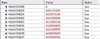
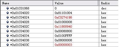
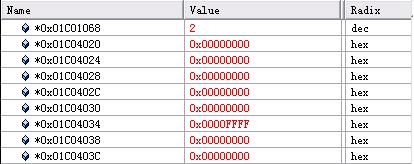
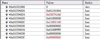
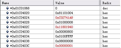
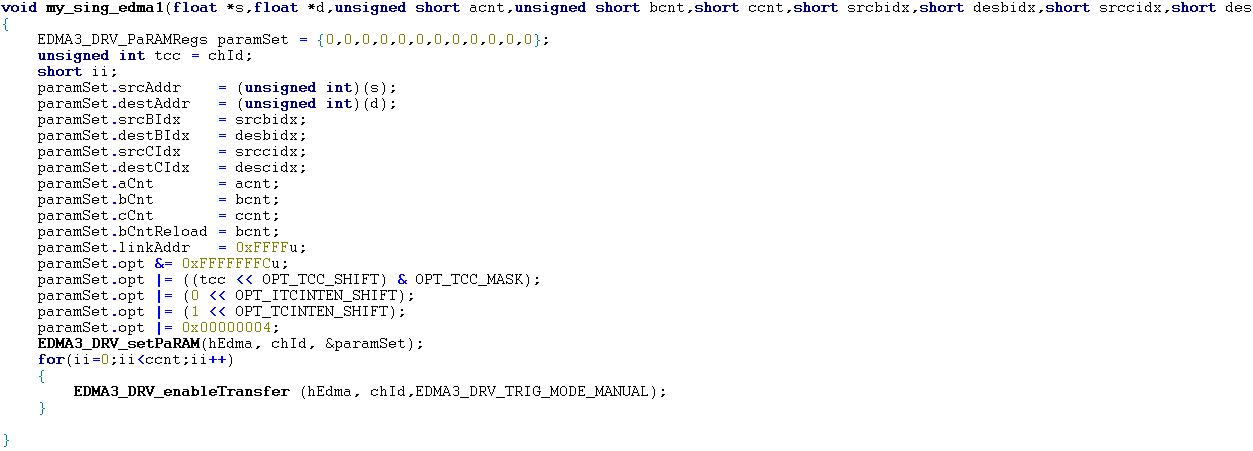
I use c6747. When I use edma, I meet a very strange problem. I want to move four columns. When the program runs, I find the first, second and third columns are moved successfully. But the fourth column isn't moved. To find the reason, I put a breakpoint on the enable transport function, and then I find all of the four columns can be moved. If I add a function of printf after the enable transport function, the four columns also can be moved without a breakpoint. I don't know why and how to reslove this problem. Can somebody help me?

  • Hi wu wu,

    Breakpoint and printf are ways which add a certain amount of delay in the program, because they take a higher amount of instruction cycles.

    So, one way could be to add a fixed amount of delay in your program. Or there could be some flag in the EDMA control / status register which you can poll/ use as an interrupt to ensure that the entire operation has been completed successfully. In this way, you dont add any random delay in your program and aslo you can monitor the speed of your operation and maybe try to optimize your code to achieve higher speeds which should be close to ideal DMA speeds.

    Hope this helps.

    Regards,

    Sid


  • Hi Sid,

             In the program, I use the IPR(Interrupt Pending Register) to monitor the transport of the data. I enable the TCINTEN bit in OPT. When the operation is processing, I want to do some other things, so I don't enable the ITCINTEN bit in OPT. If operation isn't commpleted, the program waits. Even the waiting time is long, which I think exceeds the time when there is a breakpoint, So I'm confused.

  • Welcome to the E2E Forum. There is a lot of information throughout the forum, and a lot of people who can help you and learn from you. Sid shows the breadth of resources supporting you here on the E2E Forum.

    I am going to ask a list of questions about the enable transport function, because my point-of-view is from the EDMA3 out. But my instinct tells me that Sid has the right idea, following your lead that a breakpoint before or printf after the enable transport function makes the operation complete. Sid's approach is a more system-level approach to find the cause of the problem, even if the ultimate solution will not be adding delays - first you have to discover the cause. Sid's idea to insert a long delay is a way to find out just what is causing the problem, then you can fix it after that.

    Still looking at this from the system level, what else is running in your C6747 code before and after the enable transport function is executing? Are other EDMA3 activities happening at the same time? What tells you when it is time to run the enable transport function?

    Looking at this from the EDMA3 level, here are my questions about this transfer:

    1. How are you programming the EDMA3? EDMA3 LLD, CSL, direct register accesses?
    2. Are you using a DMA or QDMA channel for the transfer?
    3. Are you using multiple PARAM sets for linking/restoring the channel that is running?
    4. What values are programmed into the 8 32-bit PARAM registers before this transfer is started? 32-bit hex values will be useful, or fully instructive code/comments.
    5. What values are in the channel's PARAM set after the failure occurs?
    6. What values are in the channel's PARAM set after operation is successful?
    7. Do you use the same DMA / QDMA channel for other transfers?
    8. When the failure occurs, do you see the IPR bit set but do not see the data moved for the 4th column, or do you not see the IPR bit set and do see the data moved, or neither the IPR bit nor the data has moved?

    Please keep us posted on your progress.

  • 1. I use EDMA3 LLD to program.

    2. using DMA.

    3. I use one PARAM set.

    4. The PARAM register set as follows:

    opt:0x00101004              srcAddr:0xC0274190                    acnt:0x008                     bcnt:0x0100                   destAddr:0x11800140                  srcBidx:0x800             destBidx:0x0008

    linkAddr:0xFFFF             bcntReload:0x0100                        srcCidx:0x0008            destCidx:0x0800           ccnt:0x0004

    5. After the failure occurs the values are the same as settings.

    6. After operation is successful, the values chang to zero except for linkAddr.

    7. No.

    8. I see both the data and the IPR bit.

    When I enable ITCINTEN and TCINTEN bit in OPT, the operation is successful. But I don't want to enable ITCINTEN bit for some reasons. I watch the SASRCBREF and DFDSTBREF values of EDMATC0 in register window, find some differences between failure and success as follows:

    ii standing for the loop number

    1. success

    ii=0               SASRCBEF=0xC02f3990    DFDSTBREF=0x11800140

    ii=1               SASRCBEF=0xC02f3998    DFDSTBREF=0x11800940

    ii=2               SASRCBEF=0xC02f39A0    DFDSTBREF=0x11801140

    ii=3               SASRCBEF=0xC02f39A8    DFDSTBREF=0x11801940

    2. failure

    SASRCBEF=0xC02f39A0    DFDSTBREF=0x11801140

    That is to say, the fourth column addresses of src and des are not in SASRCBEF and DFDSTBREF. why?

    If I modify the bcnt value which is not greater than 0x2B, the operation is succeful. Why? Is there some relationship with numbers of transfer? C6747 has four des FIFO entry. But from the values of SASRCBEF and DFDSTBREF, I have a feeling that  the last TR is not accepted.

  • Thank you for these answers back, and I have some comments and more questions:

    a. What generates the four (4) events required to complete this transaction? CPU (through ESR), external/internal peripheral event, or chaining from something else?

    b. After success and after failure, what are the values in the EDMA3CC registers EMR, ER, CER, SER, IPR?

    c. Which channel are you using? Which PARAM are you using?

    d. My question #8 was "When the failure occurs, ..." and your answer was "I see both the data and the IPR bit." I think this is not the answer you meant, but please clarify.

    e. I do not see how the answer to #5 can be correct. After each event, the PARAM srcAddr, destAddr, and ccnt values should change, so if three events occurred to cause the changes noted in your answer to #8, these PARAM registers must change, too.

    f. How, in your program, did you capture the 4 "success" lines shown in your answer to #8? Was this after an interrupt and before something else? When you do it next, please also capture the PARAM registers at those times.

    wu wu said:
    If I modify the bcnt value which is not greater than 0x2B, the operation is succeful. Why?

    This is still likely to come down to a timing issue, which is what Sid was explaining in the first reply. Shortening bcnt reduces the time for each transfer, while the breakpoint or printf increases the time available for each transfer.

  • Hi,

    Quite some progress in this thread :)

    Well, to check if this is certainly a timing issue or not, try running the program in Debug mode, do manual step wise execution first time and execute the entire program until after the concerned step, the second time .

    Manual step wise execution takes some delay and if the program runs successfully then it has got to be the timing issue.

    Hope this helps.

    Regards,

    Sid

  • Hi,

    I also think It's because of time issue. From the datasheet of c6747,  I konw the value of acnt is between 1~65535 Byte, bcnt is between 1~65535 and ccnt is also between 1~65535. In my program, the value of acnt is 8 bytes, bcnt is 512 and ccnt is 4, They are very smaller than the max number(65535 Bytes, 65535,65535).

    When the data's addresses are continous, I set acnt is 8*512 bytes,bcnt is 4 and ccnt is 1.( the data number  equals to the above setting: acnt=8 bytes, bcnt=512 and ccnt=4). In this condition, the transfer is successful.

    I don't know why time issue exists. Is there some relationship with  EDMA FIFO space?

  • I will try to help you when you have a chance to answer my questions a, b, c, and e, above.

    wu wu said:
    Is there some relationship with  EDMA FIFO space?

    Very unlikely.

    Most likely, the problem is in your system behavior or method, and with more information I will be able to help you.

  • My english is not very good, so sometimes I can't express myself exactly.

    a.  I use CPU(through ESR) to generate the four events.

    b. when it's success, the values in the EDMA3CC are: EMR=0x00,ER=0x00,CER=0x00,SER=0x00,IPR=0x02.

    when it's failure, the values in the EDMA3CC are:EMR=0x02,ER=0x00,CER=0x00,SER=0x00,IPR=0x00.

    c. I use channel 1 and paRAM 1.   The  address of paRAM 1 starts from 0x01C04020.

    d. When the failure occurs, I see neither the IPR bit nor the data(the fourth column) has moved.

    e. There are 5 pictures about successful operation: 


                                     tranfer the first column                                

                                   transfer the second column                                                                                            

                                   transfer the third column     


                                    transfer the fourth column                                                                                    

     After enabling  the channel four times, the PC point jumps from the function, and the values of IPR and paRAM change as follows:

                            after transfering all of the data

    There are one picture about failed operation. It shows values of IPR and paRAM when PC point jumps from the function:

     From the picture about failed operation, data of the fourth column don't be moved. Why it happens?

  • Not sure why the comment is there, but you express yourself very well.

    wu wu said:

    b. when it's success, the values in the EDMA3CC are: EMR=0x00,ER=0x00,CER=0x00,SER=0x00,IPR=0x02.

    when it's failure, the values in the EDMA3CC are:EMR=0x02,ER=0x00,CER=0x00,SER=0x00,IPR=0x00.

    Usually, SER is set also when EMR is set, so I am surprised that it is 0x00. But the fact the EMR = 0x02 confirms that an event was missed. This means that one of the CPU writes to ESR happened before the previous write to ESR had been serviced by the EDMA3CC Channel Controller.

    The way you have architected your transfer sequence, with CCNT=4, requires you to write to ESR 4 times. Because you do not have ITCINTEN set, there is no simple indication available to tell you when each transfer has completed. This requires you to wait an arbitrary amount of time between writes to ESR, and that amount of time is not enough.

    The simplest way to fix this is

    1. Set ITCCHEN=1 in the OPT register.
    2. Only write to ESR once, so keep the first time but remove the other 3 times that you write to ESR.

    If you want to understand how chaining works, the EDMA3 User's Guide has the details. In the Training section of TI.com, there is a training video set for the C6474. The EDMA3/QDMA/IDMA Module may help with the explanation of chaining. You can find the complete video set at http://focus.ti.com/docs/training/catalog/events/event.jhtml?sku=OLT110002 .

  • RandyP said:
      

    This means that one of the CPU writes to ESR happened before the previous write to ESR had been serviced by the EDMA3CC Channel Controller.

    C6747 has 4 des entries,so I think it can accept 4 tranfer requests at one time. Do I misunderstand the meaning of 4 entries?

    Is ESR's value  invisible? Reading ESR after writing to it, I find its value doesn't change.

  • wu wu said:
    C6747 has 4 des entries,so I think it can accept 4 tranfer requests at one time. Do I misunderstand the meaning of 4 entries?

    What is the "des entry" you are talking about? In any case, yes, you misunderstand the meaning of 4 entries.

    wu wu said:
    Is ESR's value  invisible? Reading ESR after writing to it, I find its value doesn't change.

    No, ESR's value is not invisible, although it is rare to read a non-zero value there.

    Please show the exact program snippet that you use to write to ESR four times.

    It sounds like you are writing to ESR four times in a row without waiting to see if it is ready. If I am predicting the contents of your code snippet correctly, this is where your failure occurs.

    The recommended way to execute an ABC 3-dimensional transfer is to use chaining as I described above.

    The recommended way to use multiple ESR writes to step through an ABC 3-dimensional transfer is to poll IPR for completion of each transfer. Use Early Mode if you want to improve on the ESR write rate. An example would be to use the following pseudo code:

    EDMA3 pseudo code said:
    ITCINTEN = 1; // set IPR for the first 3
    TCINTEN = 1;  // generate real interrupt for the last one
    TCCMODE = 1;  // early mode to get IPR quickly
    IER &= ~2;    // clear IER bit for now

    ESR = 2;      // assume the channel is ready now
    while ( IPR & 2 == 0 ) wait;  // wait for 1st Transfer Request to be sent to TC

    ICR = 2;      // clear IPR before writing ESR to avoid race condition
    ESR = 2;      // trigger 2nd column
    while ( IPR & 2 == 0 ) wait;  // wait for 2nd TR to be sent to TC

    ICR = 2;      // clear IPR before writing ESR to avoid race condition
    ESR = 2;      // trigger 3rd column
    while ( IPR & 2 == 0 ) wait;  // wait for 3rd TR to be sent to TC

    ICR = 2;      // clear IPR before writing ESR to avoid race condition
    TCCMODE = 0;  // use normal mode to get interrupt only when transfer is complete
    IER |= 2;     // set IER bit for interrupt
    ESR = 2;      // trigger 4th column
    // you will get an interrupt when the 4th column completes


  • There are something about entries of destination FIFO register set in the c6747's datasheet:


    Based on above, I think I think it can accept 4 tranfer requests at one time. If I misunderstand this meaning, can you tell me how to understand above information?

    I use EDMA3 LLD to program. So I don't modify some relative registers by hand but using functions provided by examples of EDMA3 LLD.

    this is my program:

            my_edma(wft,p,2*sizeof(float),256,4,512*sizeof(float),2*sizeof(float),2*sizeof(float),512*sizeof(float),1);

            while(*(unsigned int *)0x01C01068!=0x00000002);

             *(unsigne int *)0x01C01070=*(unsigne int *)0x01C01070 | 0x00000002;

    this is the function of my_edma:

          void my_edma(float *s, float *d, unsigned short acnt, unsigned short bcnt, unsigned short ccnt, short srcbidx, short desbidx, short srccidx, short descidx,unsigned short chId)

        {

             EDMA3_DRV_PaRAMRegs paramSet={0,0,0,0,0,0,0,0}

            unsigned short tcc=chId;

             short  ii;

              paramSet.srcAddr=(unsigned int)(s);

              paramSet.destAddr=(unsigned int)(d);

              paramSet.srcBidx=srcbidx;

              paramSet.destBidx=desbidx;

              paramSet.srcCidx=srccidx;

              paramSet.destCidx=descidx;

              paramSet.aCnt=acnt;

              paramSet.bCnt=bcnt;

              paramSet.cCnt=ccnt;

              paramSet.bCntReload=bcnt;

              paramSet.linkAddr=0xFFFF;

              paramSet.opt &= 0xFFFFFFFC;

              paramSet.opt  |= ((tcc << OPT_TCC_SHIFT) & OPT_TCC_MASK);

              paramSet.opt  |= (0 << OPT_ITCINTEN_SHIFT);

              paramSet.opt  |= (1 << OPT_TCINTEN_SHIFT);

              paramSet.opt  |=  0x00000004;

              EDMA3_DRV_setPaRAM(hEdma,chId,&paramSet);

              for(ii=0; ii<ccnt ;ii++)

               {

                 EDMA3_DRV_enableTransfer(hEdma, chId, EDMA3_DRV_TRIG_MODE_MANUAL);

                }

    }

       The two functions EDMA3_DRV_setPaRAM and EDMA3_DRV_enableTransfer are provide are provided by EDMA3 LLD examples. ESR is modified in EDMA3_DRV_enableTranser.

  • wu wu said:
    I think it can accept 4 tranfer requests at one time. If I misunderstand this meaning, can you tell me how to understand above information?

    I now understand that you were using the term "des entries" to refer to the "Destination FIFO register sets". Thank you for the clarification.

    If you submit the TRs correctly, you can have 4 TRs "in-flight" meaning that 4 TRs can be active in the TC at one time. But the TC can only be reading data for one (1) TR at a time. The Destination FIFO register sets are for storing data to be written, not TRs to be executed; there is a difference. And the FIFOs are limited in size, which will limit the number of TR writes that can be buffered in the FIFOs.

    The problem here is that you are not submitting the TRs correctly. Please refer to the following section from the EDMA3 UG.

    In the second paragraph, it says "the TR is submitted to the associated EDMA3TC and the channel can be triggered again." This also means that the channel cannot be triggered again until the TR is submitted to the TC". In this case, you are triggering the channel too soon, before the TR has been submitted to the TC. This is not the recommended way to trigger the channel.

    The fourth paragraph explains the exact failure that occurs here. When you trigger a channel too soon, that is while it is still in the prioritization process or while it is still in the event queue (TR has not been submitted to TC), then the ESR.En bit may not be cleared before you write to it again. When you write to ESR.En again while ESR.En=1, the event is marked as being missed and this event will not result in another event being prioritized or enqueued. Since you have seen EMR.En=1, this is the indication that this has occurred.

    The recommended way to trigger the same channel multiple times is what I outlined in my previous post using pseudo code.

    An alternative that you might prefer is the following:

    replacement code said:
              for(ii=0; ii<ccnt ;ii++)
               {
                 while(*0x01C01010 & 0x00000002);  // wait for ESR.En=0

                 EDMA3_DRV_enableTransfer(hEdma, chId, EDMA3_DRV_TRIG_MODE_MANUAL);
                }

    I have not checked this out and I do not recommend it on behalf of TI; there may be race conditions that I have not considered, just as your current method encounters the race condition described above.

    I still recommend the procedure outlined in my previous post in which you wait for the IPR bit to be set. To implement the code I outlined in the previous post, you may certainly use the EDMA3 LLD routines to implement those same functions, just as the enableTransfer function implements the write to ESR.