This thread has been locked.

If you have a related question, please click the "Ask a related question" button in the top right corner. The newly created question will be automatically linked to this question.

TDA3: Question about Power down sequence

Part Number: TDA3

Hi,

 I have questions about power down sequence, Figure 5-2. Power-Down Sequencing on TDA3x DM.

1) Note4 is written as follows:

  (4) vdd_dspeve can ramp down before or at the same time as vdd/vpp.

 What dose Vpp mean?

2) About Note7:

 (7) xi_osc0 can be turned off anytime after porz assertion and must be turned off before vdda_osc voltage rail is shutdown.

Who is tun off or control xi_osc0? xi_osc0 connects crystal. so, I can't control it.

Regards,
Kenshow

  • Hi Kenshow,

    I have forwarded your question to the DM team to comment.

    Regards,
    Yordan
  • Hi kenshow,

    DM team will respond soon. Until then:

    1. vpp was a power supply pin on earlier devices. I cannot find vpp pin in TDA3. It could be connected internally with vdd. In all cases, users must refer to vdd pin only.

    2. Note 7 should be referring to the external clock scenario (No crystal but external square clock fed to xi_osc0). With external oscillator, user can control the clock - for example disable it upon POR, etc.

    Regards,

    Stan

  • Hi Stan,

     Thank you.

    Regards,
    Kenshow
  • Hi Stan,

    I would like to confirm the meanings below.
    "they can start ramping down no sooner than 100μs after PORz low"
    Is it means they must start ramping down within 100us after PORx low?

    Regards,
    Kenshow
  • Hi Stan,

    I have additional questions.

    1) no sooner than XXXμs (This is previous question)
    "they can start ramping down no sooner than 100μs after PORz low"
    Is it means they must start ramping down within 100us after PORx low?

    2) About Note 3
    "If all vddshv_* are 1.8V, then neither vdd_dspeve or vdd should start ramping down no sooner than 100μs
    after PORz low assertion.."

    3) About Note7
    "must be turned off before vdda_osc voltage rail is shutdown"
    So, I think Note 7 of the figure is wrong. Time should be extended until vdda_osc shutdown is completed.

    Regards,
    Kenshow
  • Hi Kenshow,

    Below is my understanding. I will notify the DM team to help.

    1) POR=asserted(low) ------>Guard period (100uS)------>3.3V vddshv can ramp-down
    2) To me it is also hard to understand. I will let DM team to clarify
    3) POR=asserted(low)-------->Clock can stop(no specific delay required)--------->vdda_osc starts to ramp down
    Actually this requirement should imply to shorten the time i.e. Note 7 line should end at the earlier vertical line which in fact represents the vdda_osc point of ramp-down start.
    I think that is because the oscillator becomes unpowered and therefore no signals (clock in our case) should be input to it.

    Regards,
    Stan
  • Hi Stan,

    1) Dose the Guard period (100uS) mean max time? or min?
    2) I am waiting for you to explain the meaning of the sentence.
    3) I understood.

    Regards,
    Kenshow
  • Hi Stan,

    I have some addition questions about power down.

    4) There is no power supply of signal name "vddshv_*". Is these a signal name "vddshv*", no need under bar?
    5) About note5,
    "If vdds18v_ddr and vdds_ddr* are kept separate from vdds18v_* on board, then this combined DDR supply can come down
    together or before the vdds18v_* supply."
    What dose it means?

    Regards,
    Kenshow
  • Hi Kenshow,

    1) This is the minimum time you have to ensure before starting ramp-dawn.

    2) If all vddshv* supplies are 1.8V, then these rails can ramp down at the same time as vdds18v_*. This means they are allowed to ramp down after vdd_dspeve and vdd.
    Previous sentence explain that you must wait for the guard time before starting the ramp down process with 3.3V power supplies
    In this particular case, there is no 3.3V power supplies to start ramping down with, so you will have to start with the cores (vdd_dspeve and vdd). However you still must provide the guard period, nevertheless there is no 3.3V supplies. So you still have to wait for at least 100μs before starting to ramp down the cores.

    4)Yes, this is a typo.

    5) First bullet in note 5 explains the option when DDR2 memory is used and those supplies are combined and sourced from the same source (as DDR2 voltage is 1.8V).
    Second bulled explains that is possible also to not source those from a single source . If you keep sources for ddr (vdds_ddr1, vdds_ddr2, vdds_ddr3) and vdds18v_* (vdds18v_ddr1, vdds18v_ddr2, vdds18v_ddr3) separated, you must ensure ddr supply will never ramp down after the vdds18v_*.

    In general I would recommend you to use the dedicated PMICs for this SoC. They are supporting power sequencing requirements and other great features.

    Thanks,
    Dian
  • Hi Dian,

    Thanks for the details.

    1) I attached the figure to avoid my misunderstanding. Could you check whether it is OK?
    As same as note5, 500us is minimum time isn’t it?

    I believe that using PMIC is the best way. However, I need to know the specification of TDA3 exactly as a power designer for automotive application.

    Regards,
    Kenshow

  • Hi Kenshow,

    Not sure what is your question, but above diagrams look valid... with one note - vdds_ddr* must be ramped down before vdds18v.
    I do not see timing for vdds18v, but assume it starts ramping down after vdds_ddr*.
    In general, there are no dependencies between vdds_ddr* and vdda_* domains.

    Thanks,
    Dian
  • Dain,

    I just want to reconfirm the definition of minimum time about 100us and 500us.

    Thanks,
    Kenshow
  • Hi Dian,

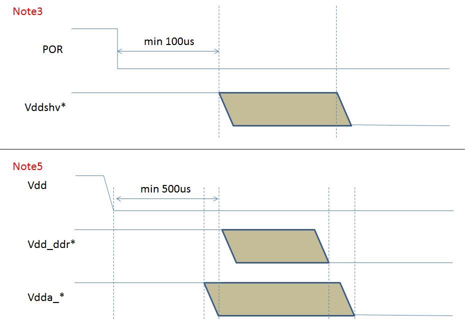
    My question is about NOT 3 and 5 of Figure 5-2. Power-Down Sequencing in DM.

    Note 3 is written "they can start ramping down no sooner than 100μs after PORz low assertion".

    Note 5 is written "vdds_ddr* can start ramping down no sooner than 500μs after vdd".

    So, I want to reconfirm about the idea of the defined time, 100us and 500us.

    Is my figure OK?

    Regards,
    Kenshow

  • Please find below further clarifications regarding Notes 3 & 5 of the TDA3x Power Down Seq diagrams.

    Note 3:

    PORz must be asserted low for 100us minimum elapsed time before any TDA3 voltages go below their minimal functional level to ensure all SoC circuitry has been set to a known safe state. If any vddshv* uses 3.3V, then this supply must remain greater than 2.7V for 100us after PORz is asserted low. If all vddshv* are set to 1.8V & using same supply source as VDDS1V8, then they can ramp down at the same time as VDDS1V8.  In this case, the 1st supplies to ramp down will be vdd & vdd_dspeve.  Niether of these supplies should begin ramping down no sooner than 100us after PORz has been asserted low to ensure TDA3 has been set to a safe state before SoC voltages begin the power down seq.

    Note 5:

    The 500us delay before disabling vdds_ddr is intended to allow vdd to begin discharging with sufficient time so that vdds_ddr supply does not ramp down more quickly than vdd.

  • Hi Bill,

    Thank you very much.

    Regards,
    Kenshow