This thread has been locked.

If you have a related question, please click the "Ask a related question" button in the top right corner. The newly created question will be automatically linked to this question.

AM3352: McASP transmit not working

Part Number: AM3352
Other Parts Discussed in Thread: SYSCONFIG,

for starters Yes i am following section 22.3.12.2 of the tech manual and i have seen this post:  

this is a TI-RTOS project on a custom board.

i am not using starterware to program the McASP, just writing to registers. here is the setup

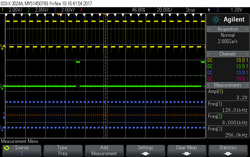
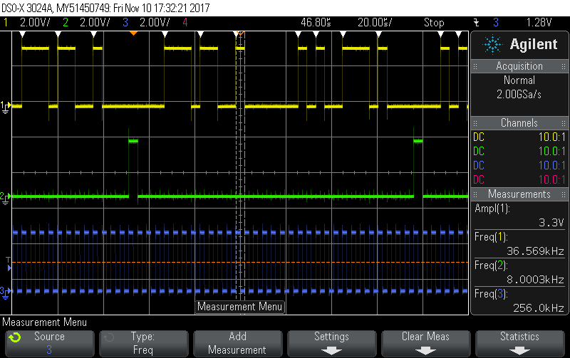
McASP0 connected to codec 320AIC3106 via pins AXR0 (receive), AXR1 (transmit), ACLKX (clock generated by the codec), and FSX (clock generated by the codec). we are running at 8KHz with 2 slots per frame, synchronous. 

i can receive just fine. i don't have any problems with that.

my transmit interrupt works just fine. i am getting all my interrupts it seems. my problem is that my pin is dead. i turned the pin into a gpio and set it and cleared it and i watched it go up and down on a scope so i know it functions. i am using serializer 1 as the transmit. i initialize this thing outside of main so interrupts are running when it turns on.

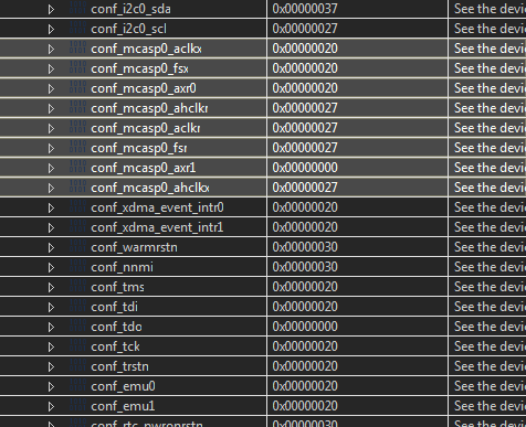
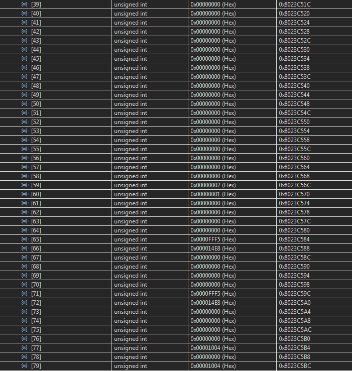
My PFUNC register is set to 0 so everything is McASP for right now. my PDIR register is set to 0x00000002 so i believe my serializer 1 pin is an output. my SRCTL_1 register is set to 0x00000001. my interrupts for XINTCTL are DATA_RDY and UNDERRUN. i am not hitting underrun. i am writing to the configuration bus so i am writing directly to serializer 1's tx register. 

i have tried setting my pinmux as both an input and an output and it didn't seem to make a difference. i am not paying attention to the CLKCHK error nor am i doing anything to set up the AHCLK, i just let them be where they are. my AMUTE register is set to 0 so errors should not cause a mute. 

are there other errors other than underrun that would cause the TX pin to not function? did i miss a note somewhere telling me out to enable a serializer pin for output?

  • The RTOS team have been notified. They will respond here.
  • what is the value of XSTAT and XGBLCTL registers?? Is XTDM set to have slot 0 and slot 1 active. Has the transmit state machine taken out of reset in GBLCTL. Do you see the transmit clock and frame sync being generated correctly on the scope.

    It would help if you post the part of MCASP transmit initialization code or compare it with either starterware or driver code:

    If you are using rCSL , here is some code for reference.
    processors.wiki.ti.com/.../QuickStartOMAPL1x_rCSL

    Regards,
    Rahul
  • the rx and tx are pretty well mirrored for settings. the clocks are working just fine and are the expected frequencies. 

    i am not using the CSL

    code is a little sloppy as i am just starting in getting this working:

    #define MCASP_PWRIDLESYSCONFIG_NO_IDLE 0x00000001

    #define MCASP_PFUNC_AFSR_GPIO (1<<31)
    #define MCASP_PFUNC_AHCLKR_GPIO (1<<30)
    #define MCASP_PFUNC_ACLKR_GPIO (1<<29)
    #define MCASP_PFUNC_AFSX_GPIO (1<<28)
    #define MCASP_PFUNC_AHCLKX_GPIO (1<<27)
    #define MCASP_PFUNC_ACLKX_GPIO (1<<26)
    #define MCASP_PFUNC_AMUTE_GPIO (1<<25)
    #define MCASP_PFUNC_AXR3_GPIO (1<<3)
    #define MCASP_PFUNC_AXR2_GPIO (1<<2)
    #define MCASP_PFUNC_AXR1_GPIO (1<<1)
    #define MCASP_PFUNC_AXR0_GPIO (1)

    #define MCASP_PDIR_AFSR_OUTPUT (1<<31)
    #define MCASP_PDIR_AHCLKR_OUTPUT (1<<30)
    #define MCASP_PDIR_ACLKR_OUTPUT (1<<29)
    #define MCASP_PDIR_AFSX_OUTPUT (1<<28)
    #define MCASP_PDIR_AHCLKX_OUTPUT (1<<27)
    #define MCASP_PDIR_ACLKX_OUTPUT (1<<26)
    #define MCASP_PDIR_AMUTE_OUTPUT (1<<25)
    #define MCASP_PDIR_AXR3_OUTPUT (1<<3)
    #define MCASP_PDIR_AXR2_OUTPUT (1<<2)
    #define MCASP_PDIR_AXR1_OUTPUT (1<<1)
    #define MCASP_PDIR_AXR0_OUTPUT (1)

    #define MCASP_PDOUT_SET_AFSR 0x80000000
    #define MCASP_PDOUT_SET_AHCLKR 0x40000000
    #define MCASP_PDOUT_SET_ACLKR 0x20000000
    #define MCASP_PDOUT_SET_AFSX 0x10000000
    #define MCASP_PDOUT_SET_AHCLKX 0x08000000
    #define MCASP_PDOUT_SET_ACLKX 0x04000000
    #define MCASP_PDOUT_SET_AMUTE 0x02000000
    #define MCASP_PDOUT_SET_AXR3 0x00000008
    #define MCASP_PDOUT_SET_AXR2 0x00000004
    #define MCASP_PDOUT_SET_AXR1 0x00000002
    #define MCASP_PDOUT_SET_AXR0 0x00000001

    #define MCASP_PDCLR_CLR_AFSR 0x80000000
    #define MCASP_PDCLR_CLR_AHCLKR 0x40000000
    #define MCASP_PDCLR_CLR_ACLKR 0x20000000
    #define MCASP_PDCLR_CLR_AFSX 0x10000000
    #define MCASP_PDCLR_CLR_AHCLKX 0x08000000
    #define MCASP_PDCLR_CLR_ACLKX 0x04000000
    #define MCASP_PDCLR_CLR_AMUTE 0x02000000
    #define MCASP_PDCLR_CLR_AXR3 0x00000008
    #define MCASP_PDCLR_CLR_AXR2 0x00000004
    #define MCASP_PDCLR_CLR_AXR1 0x00000002
    #define MCASP_PDCLR_CLR_AXR0 0x00000001

    #define MCASP_PDIN_IN_DATA_AFSR 0x80000000
    #define MCASP_PDIN_IN_DATA_AHCLKR 0x40000000
    #define MCASP_PDIN_IN_DATA_ACLKR 0x20000000
    #define MCASP_PDIN_IN_DATA_AFSX 0x10000000
    #define MCASP_PDIN_IN_DATA_AHCLKX 0x08000000
    #define MCASP_PDIN_IN_DATA_ACLKX 0x04000000
    #define MCASP_PDIN_IN_DATA_AMUTE 0x02000000
    #define MCASP_PDIN_IN_DATA_AXR3 0x00000008
    #define MCASP_PDIN_IN_DATA_AXR2 0x00000004
    #define MCASP_PDIN_IN_DATA_AXR1 0x00000002
    #define MCASP_PDIN_IN_DATA_AXR0 0x00000001

    #define MCASP_GBLCTL_TX_FS_ACTIVE (1<<12)
    #define MCASP_GBLCTL_TX_ST_MCHN_ACTIVE (1<<11)
    #define MCASP_GBLCTL_TX_UNSET_CLEAR (1<<10)
    #define MCASP_GBLCTL_TX_HIFREQ_DIV_ACTIVE (1<<9)
    #define MCASP_GBLCTL_TX_CLK_DIV_ACTIVE (1<<8)
    #define MCASP_GBLCTL_RX_FS_ACTIVE (1<<4)
    #define MCASP_GBLCTL_RX_ST_MCHN_ACTIVE (1<<3)
    #define MCASP_GBLCTL_RX_UNSET_CLEAR (1<<2)
    #define MCASP_GBLCTL_RX_HIFREQ_DIV_ACTIVE (1<<1)
    #define MCASP_GBLCTL_RX_CLK_DIV_ACTIVE (1)

    #define MCASP_RMASK_16_BIT 0x0000FFFF

    #define MCASP_RFMT_1BIT_DELAY (1<<16)
    #define MCASP_RFMT_MSB_FIRST (1<<15)
    #define MCASP_RFMT_SLOT_16_BITS (7<<4)
    #define MCASP_RFMT_READ_CFG_BUF (1<<3)

    #define MCASP_AFSRCTL_2_SLOT_TDM (2<<7)

    #define MCASP_RTDM_1_ACTIVE_TIME_SLOTS 0x00000001
    #define MCASP_RTDM_2_ACTIVE_TIME_SLOTS 0x00000003
    #define MCASP_RTDM_ALL_TIME_SLOTS_ACTIVE 0xFFFFFFFF

    #define MCASP_RINTCTL_RX_DATA_RDY_EN (1<<5)
    #define MCASP_RINTCTL_RX_CLK_FAIL_EN 0x00000004
    #define MCASP_RINTCTL_RX_SYNC_ERROR_EN 0x00000002
    #define MCASP_RINTCTL_RX_OVERRUN_EN 0x00000001

    #define MCASP_RSTAT_ERROR 0x00000100
    #define MCASP_RSTAT_DMA_ERROR 0x00000080
    #define MCASP_RSTAT_START_OF_FRAME 0x00000040
    #define MCASP_RSTAT_DATA_RDY 0x00000020
    #define MCASP_RSTAT_LAST_SLOT 0x00000010
    #define MCASP_RSTAT_EVEN_SLOT 0x00000008
    #define MCASP_RSTAT_CLOCK_FAIL 0x00000004
    #define MCASP_RSTAT_SYNC_FAIL 0x00000002
    #define MCASP_RSTAT_OVERRUN 0x00000001

    #define MCASP_XMASK_16_BIT 0x0000FFFF

    #define MCASP_XFMT_1BIT_DELAY (1<<16)
    #define MCASP_XFMT_MSB_FIRST (1<<15)
    #define MCASP_XFMT_SLOT_16_BITS (7<<4)
    #define MCASP_XFMT_WRITE_CFG_BUF (1<<3)

    #define MCASP_AFSXCTL_2_SLOT_TDM (2<<7)

    #define MCASP_XTDM_1_ACTIVE_TIME_SLOTS 0x00000001
    #define MCASP_XTDM_2_ACTIVE_TIME_SLOTS 0x00000003
    #define MCASP_XTDM_ALL_TIMESLOTS_ACTIVE 0xFFFFFFFF

    #define MCASP_XINTCTL_START_OF_FRAME_EN (1<<7)
    #define MCASP_XINTCTL_DATA_RDY_EN (1<<5)
    #define MCASP_XINTCTL_CLK_FAIL_EN (1<<2)
    #define MCASP_XINTCTL_SYNC_ERROR_EN (1<<1)
    #define MCASP_XINTCTL_UNDERRUN (1)

    #define MCASP_XCLKCHK_XMAX (10<<16)
    #define MCASP_XCLKCHK_XMIN (6<<8)

    #define MCASP_XCLKCHK_INTERNAL (1<<15)
    #define MCASP_XCLKCHK_DIVIDE_DOWN 19

    #define MCASP_XSTAT_ERROR 0x00000100
    #define MCASP_XSTAT_DMA_ERROR 0x00000080
    #define MCASP_XSTAT_START_OF_FRAME 0x00000040
    #define MCASP_XSTAT_DATA_RDY (1<<5)
    #define MCASP_XSTAT_LAST_SLOT 0x00000010
    #define MCASP_XSTAT_EVEN_SLOT 0x00000008
    #define MCASP_XSTAT_CLOCK_FAIL (1<<2)
    #define MCASP_XSTAT_SYNC_FAIL 0x00000002
    #define MCASP_XSTAT_UNDERRUN (1)

    #define MCASP_SRCTL_RRDY 0x00000020
    #define MCASP_SRCTL_XRDY 0x00000010
    #define MCASP_SRCTL_TX_EN 0x00000001
    #define MCASP_SRCTL_RX_EN 0x00000002

    void InitMcASP0(void)
    {
    Hwi_disableMIR2(HWI_MASK_MIR2_MCASP0_CODEC_TX | HWI_MASK_MIR2_MCASP0_CODEC_RX);

    //reset everything
    *MCASP0_GBLCTL = 0;

    //disable idle
    //*MCASP0_PWRIDLESYSCONFIG = MCASP_PWRIDLESYSCONFIG_NO_IDLE;

    //// INIT RX
    *MCASP0_RMASK = MCASP_RMASK_16_BIT;

    *MCASP0_RFMT = MCASP_RFMT_1BIT_DELAY | MCASP_RFMT_SLOT_16_BITS | MCASP_RFMT_READ_CFG_BUF | MCASP_RFMT_MSB_FIRST;

    *MCASP0_AFSRCTL = MCASP_AFSRCTL_2_SLOT_TDM;

    *MCASP0_ACLKRCTL = 0;

    *MCASP0_AHCLKRCTL = 0;

    *MCASP0_RTDM = MCASP_RTDM_2_ACTIVE_TIME_SLOTS;

    *MCASP0_RINTCTL = MCASP_RINTCTL_RX_DATA_RDY_EN; //don't enable error ints yet

    *MCASP0_RCLKCHK = 0;

    //// INIT TX
    *MCASP0_XMASK = MCASP_XMASK_16_BIT;

    *MCASP0_XFMT = MCASP_XFMT_1BIT_DELAY | MCASP_XFMT_SLOT_16_BITS | MCASP_XFMT_WRITE_CFG_BUF | MCASP_XFMT_MSB_FIRST;

    *MCASP0_AFSXCTL = MCASP_AFSXCTL_2_SLOT_TDM;

    *MCASP0_ACLKXCTL = 0;

    *MCASP0_AHCLKXCTL = 0; //MCASP_XCLKCHK_INTERNAL | MCASP_XCLKCHK_DIVIDE_DOWN; //based on AUXCLK, which is 19.2MHz

    *MCASP0_XTDM = MCASP_XTDM_2_ACTIVE_TIME_SLOTS;

    *MCASP0_XINTCTL = MCASP_XINTCTL_DATA_RDY_EN | MCASP_XINTCTL_UNDERRUN; //don't enable error ints yet

    *MCASP0_XCLKCHK = 0; //MCASP_XCLKCHK_XMAX | MCASP_XCLKCHK_XMIN;

    //serializers
    *MCASP0_SRCTL_0 = MCASP_SRCTL_RX_EN;
    *MCASP0_SRCTL_1 = MCASP_SRCTL_TX_EN;

    //pin configuration
    *MCASP0_PFUNC = 0;/*MCASP_PFUNC_AFSR_GPIO | MCASP_PFUNC_AHCLKR_GPIO |
    MCASP_PFUNC_ACLKR_GPIO | MCASP_PFUNC_AHCLKX_GPIO | MCASP_PFUNC_AMUTE_GPIO |
    MCASP_PFUNC_AXR3_GPIO | MCASP_PFUNC_AXR2_GPIO;*/

    *MCASP0_PDIR = MCASP_PDIR_AXR1_OUTPUT;

    //set up serializers (needed even for ext clocking)
    *MCASP0_GBLCTL |= MCASP_GBLCTL_TX_HIFREQ_DIV_ACTIVE | MCASP_GBLCTL_RX_HIFREQ_DIV_ACTIVE;
    //verify
    while((*MCASP0_GBLCTL & (MCASP_GBLCTL_TX_HIFREQ_DIV_ACTIVE | MCASP_GBLCTL_RX_HIFREQ_DIV_ACTIVE)) !=
    (MCASP_GBLCTL_TX_HIFREQ_DIV_ACTIVE | MCASP_GBLCTL_RX_HIFREQ_DIV_ACTIVE));

    Hwi_enableMIR2(HWI_MASK_MIR2_MCASP0_CODEC_TX | HWI_MASK_MIR2_MCASP0_CODEC_RX);

    //clear stat registers if you can
    *MCASP0_RSTAT = 0xFFFF;
    *MCASP0_XSTAT = 0xFFFF;

    //enable McASP
    //undo clear bits for state machine
    *MCASP0_GBLCTL |= MCASP_GBLCTL_TX_UNSET_CLEAR | MCASP_GBLCTL_RX_UNSET_CLEAR;
    //verify
    while((*MCASP0_GBLCTL & (MCASP_GBLCTL_TX_UNSET_CLEAR | MCASP_GBLCTL_RX_UNSET_CLEAR)) !=
    (MCASP_GBLCTL_TX_UNSET_CLEAR | MCASP_GBLCTL_RX_UNSET_CLEAR));

    //take state machine out of reset
    *MCASP0_GBLCTL |= MCASP_GBLCTL_TX_ST_MCHN_ACTIVE | MCASP_GBLCTL_RX_ST_MCHN_ACTIVE;
    //verify
    while((*MCASP0_GBLCTL & (MCASP_GBLCTL_TX_ST_MCHN_ACTIVE | MCASP_GBLCTL_RX_ST_MCHN_ACTIVE)) !=
    (MCASP_GBLCTL_TX_ST_MCHN_ACTIVE | MCASP_GBLCTL_RX_ST_MCHN_ACTIVE));

    //take frame sync out of reset
    *MCASP0_GBLCTL |= MCASP_GBLCTL_TX_FS_ACTIVE | MCASP_GBLCTL_RX_FS_ACTIVE;
    //verify
    while((*MCASP0_GBLCTL & (MCASP_GBLCTL_TX_FS_ACTIVE | MCASP_GBLCTL_RX_FS_ACTIVE)) !=
    (MCASP_GBLCTL_TX_FS_ACTIVE | MCASP_GBLCTL_RX_FS_ACTIVE));
    }

  • so i still don't have answer to this

    what is everything that needs to happen to get this pin to be functional?

    power domain enabled 

    Pinmux set correctly - Question - do it set it to input or output? since it CAN be configured for an input or an output inside the McASP module i would assume input, but i am using it as an output, so which is it?

    McASP pin function set to McASP pin

    McASP direction set to output

    Clocks functional

    no underrun error

    setup following instructions

    interrupts enabled

    as mentioned i am getting the interrupts and i am writing to the XBUF1 register to get the samples out, everything SEEMS to be functioning EXCEPT the pin does nothing. i have verified that i only get underrun errors when i refresh the variable that monitors it and that i am getting interrupts by filling a buffer with the sample i am trying to transmit.

  • i'm guessing that since i haven't had a response everyone else is at a loss as well
  • cobsonchael,

    Sorry for the delayed response,  I was sidetracked from this thread due some priority tasks and haven`t kept up with your responses.

    You are trying to program McASP using direct register writes instead of using functional CSL or McASP LLD driver. This will be harder to debug when we don`t have the same environment setup and don`t have full visibility of SOC Registers to comment where the issue lies. Can you provide this project in a form which we can reproduce on our EVM.  We recommend that you use Processor SDK RTOS CSL or LLD driver to program the MCASP.

    For reference CSL code, we provide a MCASP CSL code for OMAPL platform using AIC3106  in the board diagnostics that is found under:

    pdk_am335x_1_0_7\packages\ti\board\diag\mcasp\src

    you can look at the BoardDiag_McASPI2SConfigure function as defined in the mcasp_test.c.

    McASPRxReset(SOC_MCASP_CFG_BASE);
    	McASPTxReset(SOC_MCASP_CFG_BASE);
    
    	/* Enable the FIFOs for DMA transfer */
    	McASPReadFifoEnable(SOC_MCASP_CFG_BASE, 1, 1);
    	McASPWriteFifoEnable(SOC_MCASP_CFG_BASE, 1, 1);


        /* Set I2S format in the transmitter/receiver format units */
        McASPRxFmtI2SSet(SOC_MCASP_CFG_BASE, WORD_SIZE, SLOT_SIZE,
                             MCASP_RX_MODE_DMA);
        McASPTxFmtI2SSet(SOC_MCASP_CFG_BASE, WORD_SIZE, SLOT_SIZE,\
        		MCASP_TX_MODE_DMA);
    
        McASPRxFrameSyncCfg(SOC_MCASP_CFG_BASE, 2, MCASP_RX_FS_WIDTH_WORD,
                                MCASP_RX_FS_EXT_BEGIN_ON_RIS_EDGE);
        McASPTxFrameSyncCfg(SOC_MCASP_CFG_BASE, 2, MCASP_TX_FS_WIDTH_WORD,
                                MCASP_TX_FS_EXT_BEGIN_ON_RIS_EDGE);
    
        /* configure the clock for receiver */
    	McASPRxClkCfg(SOC_MCASP_CFG_BASE, MCASP_RX_CLK_EXTERNAL, 0, 0);
    	McASPRxClkPolaritySet(SOC_MCASP_CFG_BASE, MCASP_RX_CLK_POL_RIS_EDGE);
    	McASPRxClkCheckConfig(SOC_MCASP_CFG_BASE, MCASP_RX_CLKCHCK_DIV32,
    						  0x00, 0xFF);
    
        /* configure the clock for transmitter */
        McASPTxClkCfg(SOC_MCASP_CFG_BASE, MCASP_TX_CLK_EXTERNAL, 0, 0);
        McASPTxClkPolaritySet(SOC_MCASP_CFG_BASE, MCASP_TX_CLK_POL_FALL_EDGE);
        McASPTxClkCheckConfig(SOC_MCASP_CFG_BASE, MCASP_TX_CLKCHCK_DIV32,
                              0x00, 0xFF);
    
        /* Enable synchronization of RX and TX sections  */
        McASPTxRxClkSyncEnable(SOC_MCASP_CFG_BASE);
        /* Enable the transmitter/receiver slots. I2S uses 2 slots */
        McASPRxTimeSlotSet(SOC_MCASP_CFG_BASE, I2S_SLOTS);
        McASPTxTimeSlotSet(SOC_MCASP_CFG_BASE, I2S_SLOTS);
    
        /*
        ** Set the serializers
        */
    
        McASPSerializerTxSet(SOC_MCASP_CFG_BASE, MCASP_XSER_TX);
        McASPSerializerRxSet(SOC_MCASP_CFG_BASE, MCASP_XSER_RX);
    
    
        /*
        ** Configure the McASP pins
        ** Output - Frame Sync, Clock, Serializer Rx and Serializer Tx
        **          (Clocks generated internally)
        */
       McASPPinMcASPSet(SOC_MCASP_CFG_BASE, 0xFFFFFFFF);
       McASPPinDirOutputSet(SOC_MCASP_CFG_BASE, MCASP_PIN_AXR(MCASP_XSER_TX));
       McASPPinDirInputSet(SOC_MCASP_CFG_BASE, MCASP_PIN_AFSX
    											  | MCASP_PIN_ACLKX
    											  | MCASP_PIN_AFSR
    											  | MCASP_PIN_ACLKR
    											  | MCASP_PIN_AXR(MCASP_XSER_RX));
    
       /* Enable error interrupts for McASP */
       McASPTxIntEnable(SOC_MCASP_CFG_BASE, MCASP_TX_DMAERROR
    										   | MCASP_TX_CLKFAIL
    										   | MCASP_TX_SYNCERROR
    										   | MCASP_TX_UNDERRUN);
    
       McASPRxIntEnable(SOC_MCASP_CFG_BASE, MCASP_RX_DMAERROR
    										   | MCASP_RX_CLKFAIL
    										   | MCASP_RX_SYNCERROR
    										   | MCASP_RX_OVERRUN);

    Regards,

    Rahul

  • i guess i don't understand what you mean when you say "...provide this project in a form which we can reproduce on our EVM". do you mean you need the files themselves? do you need me to make a project for you?
  • I mean, can zip up your project with all relevant files so that we can run this on the EVM and look at the MCASP and system configuration register setup.
  • can i send it through email rather than publicly? also, since i don't know which EVM you are using or am familiar with that board i assume you will be responsible for filling in the gaps for things like pinmux, GPIO, codec initialization, etc?
  • is it possible to send it privately?

  • cobsonchael,

    I have forwarded the file I received from you to Rahul Prabhu.

  • cobsonchael,

    Victor has reached out to us to speed up the debug process for this issue. As I indicated earlier, debugging this issue is challenging for us as you have choosen to develop the MCASP code using register bit level configuration instead of using CSL APIs or MCASP driver APIs from Processor SDK RTOS. Due to these challenges, we have created Checklist/guidelines for getting support on software issues which are posted on Sitara forums which indicate that for support on E2E forums please develop bare-metal and RTOS code using Processor SDK RTOS. We support a wide range of customers so I hope you understand the delay in supporting such development efforts where the software as well as hardware is customized.

    Having said that I have reviewed the cutdown code that Victor has forwarded to us and had a few questions/comments:

    1. In your post you indicated that FSX and ACLKX are recieved from the codec. Can you please indicate if the MCLK is connected to the ACLKX pin clock as an input, or is ACLKX bit clock divided down from MCLK connected to AHCLKX high-frequency master clock.
    2. Can you read XSTAT after you reset the state machine and frame sync to see if there are any issues on the transmit side. If possible please provide the full MCASP register configuration from CCS register view after the you release reset by configuring GBLCTL register.
    3. In sync mode the receive clock is obtained from the transmit side so I would assume then ACLKX and ACLKR bit clocks are correctly received and internally synchronized, have you also checked the transmit frame sync using a scope.
    4. Can you invert the transmit clock polarity using CLKXP = 1 in ACLKXCTL, in the MCASP -AICCODEC examples that we provide the CLKXP seems to be set to 1 as External receiver samples data on the rising edge of the serial clock, so the transmitter must shift data out on the falling edge of the serial clock

    I will continue to look at this code tomorrow and let you know if I can recommend other debug steps.

    Regards,
    Rahul

  • 1) the codec m-clock is attached to a 24.576MHz crystal. the codec generates the frame sync (8KHz) which goes to FSX and the WCLK connected to ACLKX. we are set up for 2 16-bit words. AHCLKX is not used

    2) i am guessing you want the register view after the initialization process is complete? if not and there is a certain point in the setup process please indicate where in the setup process steps you would like the register view? as you know there are a lot of things that get released from reset inside the GBLCTL register. either way here are the registers at the end of initialization:

    XSTAT before hitting the breakpoint is 0x00000104, as hitting a breakpoint generates additional errors that wouldn't have been there otherwise. the errors are XCKFAIL which shouldn't affect anything since we don't have the system setup to check the clock, and XERR which just means there is an error

    3) ACLKR is not used, we are only connected to ACLKX. i have checked the frame sync and word clock using a scope and they are just fine. as i stated before i can receive just fine, verified by sending a known signal into the codec and graphing it in CCS using the single time graph

    4) Reversing the polarity of the clock didn't fix it. still no activity on AXR1

  • Thanks for providing the registers. One way to read XSTAT may be to read that in code and print it on UART or connect to the dap (debug subsystem port and look at the value) if halting the core is generating more errors.

    Also, the TRM indicates To transmit in I2S format, use MSB first, left aligned, and also select XDATDLY = 01 (Refer Table 22-9). I am curious why you have commented out the 1 bit delay bit in your setup.

    I checked for commonly known issues indicated here :
    processors.wiki.ti.com/.../McASP_Tips

    Your port configuration is consistent with your XFMT configuration, as you are setting XBUSEL =1 and you write data to XBUF but you may need to look at the 32 bit access requirement for MCASP as your configuration requires 16 bit transmit.  Your 16-bit data needs to transferred to XBUF as a  32-bit word, i.e. turn your array of uint16_t data into a uint32_t array with padding on each word

    Regards
    Rahul

  • i am reading XSTAT in code, that is how i am able to get you the value before the breakpoint. we do not have a UART connection to anything that can print it out.

    we are not using I2S format we are using TDM. the one bit delay is something i was playing with for the codec. the codec has a programmable delay and the McASP has a programmable delay. i was trying one vs the other to see if that might fix anything. surprise, it did not.

    sure, i'll change it to a 32 bit variable when i read/write
  • i haven't heard anything in a while. just wanted to make sure this is still being worked on
  • cobsonchael,

    Did you update the code to 32 bit access and try the suggestions on the wiki. What option have you used : padding the data or enabling the AFIFO?

    As I have indicated, your MCASP code is not following the support guidelines that we have provided here to us either CSL or LLD drivers for accessing the peripherals. Also you are testing this on a custom hardware that we don`t understand completely. Is there a way you can help us reproduce the issue on TI evaluation platform.

    Regards,

    Rahul

  • yes i switched to a 32 bit variable to write and read from the data registers. it made no difference.

    i will try to use the drivers. i will let you know if it fixes anything or if i have any question on how to use it

  • so right off the bat i have some questions on the McASP driver

    on the wiki 

    it states that i need to call  int32_t mcaspInit (void) to start initializing the module. when i look up that routine in the actual code/drivers, that isn't the correct prototype. the drivers have it as void mcaspInit(uint32_t instNum). in addition when i try to include it in my code i get an implicit function warning even though i included the driver.h file like the wiki told me to. AND THEN when i look at the example project that routine doesn't even get called. an entirely different method is used.  i understand i am supposed to follow the example project but what is the point of the online wiki if it isn't accurate?

  • cobsonchael,

    Sorry for this misrepresentation & thanks for bringing this to notice. We have removed the confusing mcaspInit() API from the mcasp_drv.h and moved the MCASP_deviceInit() to the mcasp_soc.h in the upcoming 4.1 release (This issue is already being tracked using bug ID PRSDK-2882). We will update the wiki accordingly.

    Regards,
    Rahul

  • the example doesn't help. it doesn't show me how to change any of the McASP settings (which serializers, what format, clock source, etc) (i found it, nevermind). it is also confusing

    the example calls McaspDevice_init which sets up Mcasp_module and Mcasp_deviceInstInfo. then it calls configMcASP_SocHwInfo which only seems to get the cfg, and send it back in:
    Mcasp_socGetInitCfg(MCASP_NUM, &hwInfo);


    /* Change anything if needed */
    Mcasp_socSetInitCfg(MCASP_NUM,&hwInfo);

    so i go to change any settings in the hwInfo settings and i find out it is the same datatype as Mcasp_deviceInstInfo, which was already set up. so what is the point of setting up Mcasp_deviceInstInfo? are those settings meant to go into hwInfo and Mcasp_socSetInitCfg? what is the point of doing a get and a set but not changing anything? i don't understand the point of McaspDevice_init if those settings are not sent to the module.

    is there another example that i can look at that might clear these things up for me? i have looked at the MCASP_LLD_SDS document but considering it is wrong at the first use of the driver API (page 11) i don't know how much of that document i can trust

    FYI your wiki fix only fixed one instance of mcaspInit , it is still there under the driver configuration section

  • The MCASP driver uses the default setup for the driver using the values used in the mcasp_soc.c. The Mcasp_socGetInitCf and Mcasp_socSetInitCfg are used to change these default settings. For example the soc configuration uses Interrupt number 80 and 81 for MCASP0 TX And RX and Interrupt number 82 and 83 for MCASP1. you can modify the interrupt setup by getting the default SOC configuration and modifying it and then using the Mcasp_socSetInitCfg. As the comment indicates, users can indicate changes to the configuration between the Mcasp_socGetInitCfg and Mcasp_socSetInitCfg calls.

    The main MCASP receive side setup and transmit side setup is provided in the mcasp_cfg.c file, that provide the mcaspRcvSetup and mcaspXmtSetup. Check the file MCASP_DeviceLoopback_evmAM335x_armExampleProject.txt in the folder to see all the source files corresponding to this example. The best way to read the code is to generate the CCS project and import it in CCS. These are the only MCASP examples that we have for this device.

    There is another MCASP project for OMAPL137, that is based on CSL which can be referred to if the intent is to look at the MCASP configuration sequence. This can be found here(pdk_am335x_1_0_7\packages\ti\board\diag\mcasp\src)

    Regards,
    Rahul
  • i get that it uses the default configuration, but what is the point of Mcasp_deviceInstInfo if it changes/sets some variable locally but never calls a routine to apply it to the McASP configuration? it seems to just set local variables but then does nothing with it, then another routine gets called that seems like it lets you get and change those SAME variables but then nothing is done with that. so what is the point of Mcasp_deviceInstInfo?
  • cobsonchael,

    The McASP driver does use this structure to setup the interrupts and to bind the driver to the device. Please refer to the source for the mcaspBindDev and mcaspRegisterInt. both those APIs will setup the driver based on information setup by the application developer using Mcasp_deviceInstInfo

    Hope this clarifies the usage.

    Regards,
    Rahul
  • Cobsonchael,

    I am picking this up from where we left this debug. We discussed this issue based on the information you have shared on the wiki so far and have a list of question to help us understand your setup and configuration. At the moment, our primary suspect is the pinmux setup as the MCASP seems to think that it is transmitting data and you are getting the transmit interrupt.

    1. Can you indicate, when you configured the Pin as an GPIO, if you used MCASP PFUNC register or the global PAD CONTROL register. Can you confirm that you generated the Pinmux using the TI pinmux tool and not using manual configuration.
    2. Please provide a register dump of the PINMUX for the FSYNC , transmit serializer and the transmit clock pin (ACLKX) and confirm that the INPUTENABLE is set to 1 for clock and frame sync
    3. Have you looked at the setup and hold time from the codec. there was a reported case of MCASP slave where the frame sync setup/hold times was causing a similar issue:
    e2e.ti.com/.../1607710
    4. Is it possiible for you to try frame sync of single word width instead of current single bit wide with your setup?


    Regards,
    Rahul
  • ok i'm back on this project again

    1) when i configured the pin as a GPIO and watched it go up and down i was doing it through the McASP GPIO controls. i did figure out my pinmux using the pinmux tool.

    2) you have my project so you can look up my pinmux code. but in case you deleted it here is my pinmux setup:

    *((U32 *)(PINMUX_BASE + 0x1d0)) = ( PIN_INPUT | MUX_MODE0 ); /* (C11) TMS.TMS */
    *((U32 *)(PINMUX_BASE + 0x1d4)) = ( PIN_INPUT | MUX_MODE0 ); /* (B11) TDI.TDI */
    *((U32 *)(PINMUX_BASE + 0x1d8)) = ( PIN_OUTPUT | MUX_MODE0 ); /* (A11) TDO.TDO */
    *((U32 *)(PINMUX_BASE + 0x1dc)) = ( PIN_INPUT | MUX_MODE0 ); /* (A12) TCK.TCK */
    *((U32 *)(PINMUX_BASE + 0x1e0)) = ( PIN_INPUT | MUX_MODE0 ); /* (B10) nTRST.nTRST */
    *((U32 *)(PINMUX_BASE + 0x1e4)) = ( PIN_INPUT | MUX_MODE0 ); /* (C14) EMU0.EMU0 */
    *((U32 *)(PINMUX_BASE + 0x1e8)) = ( PIN_INPUT | MUX_MODE0 ); /* (B14) EMU1.EMU1 */

    *((U32 *)(PINMUX_BASE + 0x88)) = ( PIN_INPUT_PULLUP | MUX_MODE7 ); /* (T13) gpmc_csn3.gpio2[0] */
    *((U32 *)(PINMUX_BASE + 0x8c)) = ( PIN_INPUT_PULLDOWN | MUX_MODE7 ); /* (V12) gpmc_clk.gpio2[1] */
    *((U32 *)(PINMUX_BASE + 0x90)) = ( PIN_INPUT_PULLUP | MUX_MODE7 ); /* (R7) gpmc_advn_ale.gpio2[2] */
    *((U32 *)(PINMUX_BASE + 0x94)) = ( PIN_OUTPUT | MUX_MODE7 ); /* (T7) gpmc_oen_ren.gpio2[3] */
    *((U32 *)(PINMUX_BASE + 0x98)) = ( PIN_INPUT_PULLDOWN | MUX_MODE7 ); /* (U6) gpmc_wen.gpio2[4] */
    *((U32 *)(PINMUX_BASE + 0x9c)) = ( PIN_INPUT_PULLUP | MUX_MODE7 ); /* (T6) gpmc_be0n_cle.gpio2[5] */
    *((U32 *)(PINMUX_BASE + 0x134)) = ( PIN_INPUT_PULLDOWN | MUX_MODE7 ); /* (L17) gmii1_rxd3.gpio2[18] */
    *((U32 *)(PINMUX_BASE + 0x138)) = ( PIN_INPUT_PULLUP | MUX_MODE7 ); /* (L16) gmii1_rxd2.gpio2[19] */
    *((U32 *)(PINMUX_BASE + 0x13c)) = ( PIN_INPUT_PULLUP | MUX_MODE7 ); /* (L15) gmii1_rxd1.gpio2[20] */
    *((U32 *)(PINMUX_BASE + 0x140)) = ( PIN_INPUT_PULLUP | MUX_MODE7 ); /* (M16) gmii1_rxd0.gpio2[21] */

    *((U32 *)(PINMUX_BASE + 0x164)) = ( PIN_INPUT | MUX_MODE7 ); /* (C18) eCAP0_in_PWM0_out.gpio0[7] */
    *((U32 *)(PINMUX_BASE + 0x11c)) = ( PIN_INPUT | MUX_MODE7 ); /* (J18) gmii1_txd3.gpio0[16] */
    *((U32 *)(PINMUX_BASE + 0x120)) = ( PIN_INPUT | MUX_MODE7 ); /* (K15) gmii1_txd2.gpio0[17] */
    *((U32 *)(PINMUX_BASE + 0x124)) = ( PIN_INPUT | MUX_MODE7 ); /* (K16) gmii1_txd1.gpio0[21] */
    *((U32 *)(PINMUX_BASE + 0x20)) = ( PIN_INPUT | MUX_MODE7 ); /* (U10) gpmc_ad8.gpio0[22] */
    *((U32 *)(PINMUX_BASE + 0x24)) = ( PIN_INPUT | MUX_MODE7 ); /* (T10) gpmc_ad9.gpio0[23] */
    *((U32 *)(PINMUX_BASE + 0x28)) = ( PIN_INPUT | MUX_MODE7 ); /* (T11) gpmc_ad10.gpio0[26] */
    *((U32 *)(PINMUX_BASE + 0x2c)) = ( PIN_INPUT | MUX_MODE7 ); /* (U12) gpmc_ad11.gpio0[27] */
    *((U32 *)(PINMUX_BASE + 0x144)) = ( PIN_INPUT_PULLUP | MUX_MODE7 ); /* (H18) rmii1_ref_clk.gpio0[29] */

    *((U32 *)(PINMUX_BASE + 0x0)) = ( PIN_INPUT | MUX_MODE7 ); /* (U7) gpmc_ad0.gpio1[0] */
    *((U32 *)(PINMUX_BASE + 0x4)) = ( PIN_INPUT | MUX_MODE7 ); /* (V7) gpmc_ad1.gpio1[1] */
    *((U32 *)(PINMUX_BASE + 0x8)) = ( PIN_INPUT | MUX_MODE7 ); /* (R8) gpmc_ad2.gpio1[2] */
    *((U32 *)(PINMUX_BASE + 0xc)) = ( PIN_INPUT | MUX_MODE7 ); /* (T8) gpmc_ad3.gpio1[3] */
    *((U32 *)(PINMUX_BASE + 0x10)) = ( PIN_INPUT | MUX_MODE7 ); /* (U8) gpmc_ad4.gpio1[4] */
    *((U32 *)(PINMUX_BASE + 0x14)) = ( PIN_INPUT | MUX_MODE7 ); /* (V8) gpmc_ad5.gpio1[5] */
    *((U32 *)(PINMUX_BASE + 0x18)) = ( PIN_INPUT | MUX_MODE7 ); /* (R9) gpmc_ad6.gpio1[6] */
    *((U32 *)(PINMUX_BASE + 0x1c)) = ( PIN_INPUT | MUX_MODE7 ); /* (T9) gpmc_ad7.gpio1[7] */
    *((U32 *)(PINMUX_BASE + 0x170)) = ( PIN_INPUT | MUX_MODE7 ); /* (E15) uart0_rxd.gpio1[10] */
    *((U32 *)(PINMUX_BASE + 0x30)) = ( PIN_INPUT | MUX_MODE7 ); /* (T12) gpmc_ad12.gpio1[12] */
    *((U32 *)(PINMUX_BASE + 0x34)) = ( PIN_INPUT | MUX_MODE7 ); /* (R12) gpmc_ad13.gpio1[13] */
    *((U32 *)(PINMUX_BASE + 0x38)) = ( PIN_INPUT | MUX_MODE7 ); /* (V13) gpmc_ad14.gpio1[14] */
    *((U32 *)(PINMUX_BASE + 0x3c)) = ( PIN_INPUT | MUX_MODE7 ); /* (U13) gpmc_ad15.gpio1[15] */
    *((U32 *)(PINMUX_BASE + 0x44)) = ( PIN_INPUT | MUX_MODE7 ); /* (V14) gpmc_a1.gpio1[17] */
    *((U32 *)(PINMUX_BASE + 0x48)) = ( PIN_INPUT | MUX_MODE7 ); /* (U14) gpmc_a2.gpio1[18] */
    *((U32 *)(PINMUX_BASE + 0x4c)) = ( PIN_INPUT | MUX_MODE7 ); /* (T14) gpmc_a3.gpio1[19] */
    *((U32 *)(PINMUX_BASE + 0x58)) = ( PIN_INPUT | MUX_MODE7 ); /* (U15) gpmc_a6.gpio1[22] */
    *((U32 *)(PINMUX_BASE + 0x5c)) = ( PIN_INPUT | MUX_MODE7 ); /* (T15) gpmc_a7.gpio1[23] */
    *((U32 *)(PINMUX_BASE + 0x60)) = ( PIN_INPUT | MUX_MODE7 ); /* (V16) gpmc_a8.gpio1[24] */
    *((U32 *)(PINMUX_BASE + 0x64)) = ( PIN_INPUT | MUX_MODE7 ); /* (U16) gpmc_a9.gpio1[25] */
    *((U32 *)(PINMUX_BASE + 0x78)) = ( PIN_INPUT | MUX_MODE7 ); /* (U18) gpmc_be1n.gpio1[28] */
    *((U32 *)(PINMUX_BASE + 0x7c)) = ( PIN_INPUT | MUX_MODE7 ); /* (V6) gpmc_csn0.gpio1[29] */
    *((U32 *)(PINMUX_BASE + 0x80)) = ( PIN_INPUT | MUX_MODE7 ); /* (U9) gpmc_csn1.gpio1[30] */
    *((U32 *)(PINMUX_BASE + 0x84)) = ( PIN_INPUT | MUX_MODE7 ); /* (V9) gpmc_csn2.gpio1[31] */

    *((U32 *)(PINMUX_BASE + 0x114)) = ( PIN_INPUT | MUX_MODE7 ); /* (J16) gmii1_txen.gpio3[3] */
    *((U32 *)(PINMUX_BASE + 0x118)) = ( PIN_INPUT | MUX_MODE7 ); /* (J17) gmii1_rxdv.gpio3[4] */
    *((U32 *)(PINMUX_BASE + 0x188)) = ( PIN_INPUT_PULLUP | MUX_MODE7 ); /* (C17) I2C0_SDA.gpio3[5] */
    *((U32 *)(PINMUX_BASE + 0x18c)) = ( PIN_INPUT | MUX_MODE7 ); /* (C16) I2C0_SCL.gpio3[6] */
    *((U32 *)(PINMUX_BASE + 0x12c)) = ( PIN_INPUT | MUX_MODE7 ); /* (K18) gmii1_txclk.gpio3[9] */
    *((U32 *)(PINMUX_BASE + 0x130)) = ( PIN_INPUT | MUX_MODE7 ); /* (L18) gmii1_rxclk.gpio3[10] */
    *((U32 *)(PINMUX_BASE + 0x234)) = ( PIN_INPUT | MUX_MODE7 ); /* (F15) USB1_DRVVBUS.gpio3[13] */
    *((U32 *)(PINMUX_BASE + 0x19c)) = ( PIN_INPUT | MUX_MODE7 ); /* (C12) mcasp0_ahclkr.gpio3[17] */
    *((U32 *)(PINMUX_BASE + 0x1a0)) = ( PIN_INPUT | MUX_MODE7 ); /* (B12) mcasp0_aclkr.gpio3[18] */
    *((U32 *)(PINMUX_BASE + 0x1a4)) = ( PIN_INPUT | MUX_MODE7 ); /* (C13) mcasp0_fsr.gpio3[19] */
    *((U32 *)(PINMUX_BASE + 0x1ac)) = ( PIN_INPUT | MUX_MODE7 ); /* (A14) mcasp0_ahclkx.gpio3[21] */

    *((U32 *)(PINMUX_BASE + 0x190)) = ( PIN_INPUT | MUX_MODE0 ); /* (A13) mcasp0_aclkx.mcasp0_aclkx */
    *((U32 *)(PINMUX_BASE + 0x194)) = ( PIN_INPUT | MUX_MODE0 ); /* (B13) mcasp0_fsx.mcasp0_fsx */
    *((U32 *)(PINMUX_BASE + 0x198)) = ( PIN_INPUT | MUX_MODE0 ); /* (D12) mcasp0_axr0.mcasp0_axr0 */
    *((U32 *)(PINMUX_BASE + 0x1a8)) = ( PIN_INPUT | MUX_MODE0 ); /* (D13) mcasp0_axr1.mcasp0_axr1 */

    *((U32 *)(PINMUX_BASE + 0x10c)) = ( PIN_INPUT | MUX_MODE4 ); /* (H17) gmii1_crs.mcasp1_aclkx */
    *((U32 *)(PINMUX_BASE + 0x110)) = ( PIN_INPUT | MUX_MODE4 ); /* (J15) gmii1_rxer.mcasp1_fsx */
    *((U32 *)(PINMUX_BASE + 0x128)) = ( PIN_INPUT | MUX_MODE3 ); /* (K17) gmii1_txd0.mcasp1_axr2 */
    *((U32 *)(PINMUX_BASE + 0x144)) = ( PIN_INPUT | MUX_MODE4 ); /* (H18) rmii1_refclk.mcasp1_axr3 */

    *((U32 *)(PINMUX_BASE + 0x14c)) = ( PIN_OUTPUT | MUX_MODE0 ); /* (M18) mdio_clk.mdio_clk */
    *((U32 *)(PINMUX_BASE + 0x148)) = ( PIN_INPUT | MUX_MODE0 ); /* (M17) mdio_data.mdio_data */

    *((U32 *)(PINMUX_BASE + 0x1b0)) = ( PIN_INPUT | MUX_MODE0 ); /* (A15) xdma_event_intr0.xdma_event_intr0 */
    *((U32 *)(PINMUX_BASE + 0x1b4)) = ( PIN_INPUT | MUX_MODE0 ); /* (D14) xdma_event_intr1.xdma_event_intr1 */

    *((U32 *)(PINMUX_BASE + 0x174)) = ( PIN_OUTPUT | MUX_MODE4 ); /* (E16) uart0_txd.eCAP1_in_PWM1_out */

    *((U32 *)(PINMUX_BASE + 0xe0)) = ( PIN_OUTPUT | MUX_MODE0 ); /* (U5) lcd_vsync.lcd_vsync */
    *((U32 *)(PINMUX_BASE + 0xe4)) = ( PIN_OUTPUT | MUX_MODE0 ); /* (R5) lcd_hsync.lcd_hsync */
    *((U32 *)(PINMUX_BASE + 0xe8)) = ( PIN_OUTPUT | MUX_MODE0 ); /* (V5) lcd_pclk.lcd_pclk */
    *((U32 *)(PINMUX_BASE + 0xec)) = ( PIN_OUTPUT | MUX_MODE0 ); /* (R6) lcd_ac_bias_en.lcd_ac_bias_en */
    *((U32 *)(PINMUX_BASE + 0xa0)) = ( PIN_OUTPUT | MUX_MODE0 ); /* (R1) lcd_data0.lcd_data0 */
    *((U32 *)(PINMUX_BASE + 0xa4)) = ( PIN_OUTPUT | MUX_MODE0 ); /* (R2) lcd_data1.lcd_data1 */
    *((U32 *)(PINMUX_BASE + 0xa8)) = ( PIN_OUTPUT | MUX_MODE0 ); /* (R3) lcd_data2.lcd_data2 */
    *((U32 *)(PINMUX_BASE + 0xac)) = ( PIN_OUTPUT | MUX_MODE0 ); /* (R4) lcd_data3.lcd_data3 */
    *((U32 *)(PINMUX_BASE + 0xb0)) = ( PIN_OUTPUT | MUX_MODE0 ); /* (T1) lcd_data4.lcd_data4 */
    *((U32 *)(PINMUX_BASE + 0xb4)) = ( PIN_OUTPUT | MUX_MODE0 ); /* (T2) lcd_data5.lcd_data5 */
    *((U32 *)(PINMUX_BASE + 0xb8)) = ( PIN_OUTPUT | MUX_MODE0 ); /* (T3) lcd_data6.lcd_data6 */
    *((U32 *)(PINMUX_BASE + 0xbc)) = ( PIN_OUTPUT | MUX_MODE0 ); /* (T4) lcd_data7.lcd_data7 */
    *((U32 *)(PINMUX_BASE + 0xc0)) = ( PIN_OUTPUT | MUX_MODE0 ); /* (U1) lcd_data8.lcd_data8 */
    *((U32 *)(PINMUX_BASE + 0xc4)) = ( PIN_OUTPUT | MUX_MODE0 ); /* (U2) lcd_data9.lcd_data9 */
    *((U32 *)(PINMUX_BASE + 0xc8)) = ( PIN_OUTPUT | MUX_MODE0 ); /* (U3) lcd_data10.lcd_data10 */
    *((U32 *)(PINMUX_BASE + 0xcc)) = ( PIN_OUTPUT | MUX_MODE0 ); /* (U4) lcd_data11.lcd_data11 */
    *((U32 *)(PINMUX_BASE + 0xd0)) = ( PIN_OUTPUT | MUX_MODE0 ); /* (V2) lcd_data12.lcd_data12 */
    *((U32 *)(PINMUX_BASE + 0xd4)) = ( PIN_OUTPUT | MUX_MODE0 ); /* (V3) lcd_data13.lcd_data13 */
    *((U32 *)(PINMUX_BASE + 0xd8)) = ( PIN_OUTPUT | MUX_MODE0 ); /* (V4) lcd_data14.lcd_data14 */
    *((U32 *)(PINMUX_BASE + 0xdc)) = ( PIN_OUTPUT | MUX_MODE0 ); /* (T5) lcd_data15.lcd_data15 */

    *((U32 *)(PINMUX_BASE + 0x70)) = ( PIN_INPUT | MUX_MODE3 ); /* (T17) gpmc_wait0.rmii2_crs_dv */
    *((U32 *)(PINMUX_BASE + 0x74)) = ( PIN_INPUT | MUX_MODE3 ); /* (U17) gpmc_wpn.rmii2_rxer */
    *((U32 *)(PINMUX_BASE + 0x40)) = ( PIN_OUTPUT | MUX_MODE3 ); /* (R13) gpmc_a0.rmii2_txen */
    *((U32 *)(PINMUX_BASE + 0x54)) = ( PIN_OUTPUT | MUX_MODE3 ); /* (V15) gpmc_a5.rmii2_txd0 */
    *((U32 *)(PINMUX_BASE + 0x50)) = ( PIN_OUTPUT | MUX_MODE3 ); /* (R14) gpmc_a4.rmii2_txd1 */
    *((U32 *)(PINMUX_BASE + 0x6c)) = ( PIN_INPUT | MUX_MODE3 ); /* (V17) gpmc_a11.rmii2_rxd0 */
    *((U32 *)(PINMUX_BASE + 0x68)) = ( PIN_INPUT | MUX_MODE3 ); /* (T16) gpmc_a10.rmii2_rxd1 */
    *((U32 *)(PINMUX_BASE + 0x108)) = ( PIN_INPUT | MUX_MODE1 ); /* (H16) gmii1_col.rmii2_refclk */

    *((U32 *)(PINMUX_BASE + 0x100)) = ( PIN_OUTPUT | MUX_MODE0 ); /* (G17) mmc0_clk.mmc0_clk */
    *((U32 *)(PINMUX_BASE + 0x104)) = ( PIN_OUTPUT | MUX_MODE0 ); /* (G18) mmc0_cmd.mmc0_cmd */
    *((U32 *)(PINMUX_BASE + 0xfc)) = ( PIN_INPUT | MUX_MODE0 ); /* (G16) mmc0_dat0.mmc0_dat0 */
    *((U32 *)(PINMUX_BASE + 0xf8)) = ( PIN_INPUT | MUX_MODE0 ); /* (G15) mmc0_dat1.mmc0_dat1 */
    *((U32 *)(PINMUX_BASE + 0xf4)) = ( PIN_INPUT | MUX_MODE0 ); /* (F18) mmc0_dat2.mmc0_dat2 */
    *((U32 *)(PINMUX_BASE + 0xf0)) = ( PIN_INPUT | MUX_MODE0 ); /* (F17) mmc0_dat3.mmc0_dat3 */

    *((U32 *)(PINMUX_BASE + 0x16c)) = ( PIN_INPUT | MUX_MODE3 ); /* (E17) uart0_rtsn.I2C1_SCL */
    *((U32 *)(PINMUX_BASE + 0x168)) = ( PIN_INPUT | MUX_MODE3 ); /* (E18) uart0_ctsn.I2C1_SDA */

    *((U32 *)(PINMUX_BASE + 0x21c)) = ( PIN_OUTPUT | MUX_MODE0 ); /* (F16) USB0_DRVVBUS.USB0_DRVVBUS */

    *((U32 *)(PINMUX_BASE + 0x150)) = ( PIN_INPUT | MUX_MODE0 ); /* (A17) spi0_sclk.spi0_sclk */
    *((U32 *)(PINMUX_BASE + 0x154)) = ( PIN_OUTPUT | MUX_MODE0 ); /* (B17) spi0_d0.spi0_d0 */
    *((U32 *)(PINMUX_BASE + 0x158)) = ( PIN_INPUT | MUX_MODE0 ); /* (B16) spi0_d1.spi0_d1 */
    *((U32 *)(PINMUX_BASE + 0x15c)) = ( PIN_OUTPUT | MUX_MODE0 ); /* (A16) spi0_cs0.spi0_cs0 */
    *((U32 *)(PINMUX_BASE + 0x160)) = ( PIN_OUTPUT | MUX_MODE0 ); /* (C15) spi0_cs1.spi0_cs1 */

    *((U32 *)(PINMUX_BASE + 0x180)) = ( PIN_INPUT | MUX_MODE0 ); /* (D16) uart1_rxd.uart1_rxd */
    *((U32 *)(PINMUX_BASE + 0x184)) = ( PIN_OUTPUT | MUX_MODE0 ); /* (D15) uart1_txd.uart1_txd */
    *((U32 *)(PINMUX_BASE + 0x178)) = ( PIN_INPUT | MUX_MODE0 ); /* (D18) uart1_ctsn.uart1_ctsn */
    *((U32 *)(PINMUX_BASE + 0x17c)) = ( PIN_OUTPUT | MUX_MODE0 ); /* (D17) uart1_rtsn.uart1_rtsn */

    where:

    #define PINMUX_BASE                 ( CONTROL_BASE + 0x800 )

    #define CONTROL_BASE                0x44E10000

    #define PIN_INPUT 0x00000020
    #define PIN_OUTPUT 0x00000000
    #define PIN_INPUT_PULLUP 0x00000030
    #define PIN_INPUT_PULLDOWN 0x00000020
    #define PIN_PULL_DISABLE 0x00000008
    #define MUX_MODE0 0x00000000
    #define MUX_MODE1 0x00000001
    #define MUX_MODE2 0x00000002
    #define MUX_MODE3 0x00000003
    #define MUX_MODE4 0x00000004
    #define MUX_MODE5 0x00000005
    #define MUX_MODE6 0x00000006
    #define MUX_MODE7 0x00000007

    unfortunately the saved pinmux file that we used to create this setup will no longer load into the pinmux utility. my pins for AXR0, AXR1, ACLKX and FSX for McASP0 are inputs

    3) i will take a look at the set up and hold time for the codec but i don't know what i am going to do if they don't match up

    4) i am using the 320AIC3106 codec as the master and unfortunately it doesn't have that option for a frame sync (that i could find). did i mention that the receive works for both channels?

  • 3) i looked at the setup and hold time for the codec vs the McASP and things look like they should apply fine. the min time for the master (codec) is longer than the min time for the slave (McASP). i would honestly be surprised if a TI codec didn't work with a TI processor anyway
  • Can you post a screenshot of the clock and frame sync so I can have a second look?

  • McASP captures.ziphere is a collection of screens from our scope.  1 is FS, 2 is bit clock, 3 is transmit, 4 is rx. as you can see RX is fine and TX does nothing

    shots 5 and 6 are the first FS bursts from the codec. 3 and 4 and close ups of the FS edge, 1 and 2 just show an overview of how it looks

    if you need the timings from the datasheets and you want screenshots of that well you can find those in the datasheet for the 3352 (page 211 sections 7.11.2)  and the 320AIC3106 datasheet (page 10 sections 9.6)

    is it possible that i am not handling underrun situations correctly? i capture them in the HWI for the McASP TX interrupt, i set a boolean to reset the peripheral, in a task (level 1) i act on that boolean by disabling the interrupts for the RX and TX (Hwi_disableMIR2(HWI_MASK_MIR2_MCASP0_CODEC_TX | HWI_MASK_MIR2_MCASP0_CODEC_RX);) and run the same init function again. this always gets my interrupts started again but no activity on the tx line

    #define HWI_MASK_MIR2_MCASP0_CODEC_TX (1<<(80-64))
    #define HWI_MASK_MIR2_MCASP0_CODEC_RX (1<<(81-64))

  • How do you currently have CLKXP configured?  I see you tried changing it at one point without luck, but from your timings it is clear that CLKXP=0 will badly violate the timing requirements.  You MUST use CLKXP=1.  In my opinion, this is clearly an issue, though perhaps the first of multiple issues.  We need to make this change and do further analysis.

  • Additionally I recommend using the I2S transfer mode of the AIC3106. It looks like you're currently using "DSP mode".
  • yes i have CLKXP configured as CLKXP = 1. remember, the codec generates the WCLK and BCLK in our project

    find all the problems possible. i would love to get this figured out and i am certainly not an expert.

    DSP or I2S, i would imagine i should be able to get it to work either way. i'll look into I2S after we figure out what's wrong with this pin

  • Please provide an updated register dump.
  • i tried I2S mode and got the same result

  • Hi cobsonchael,

    I got some time to look into this thread, but I found no smoking gun yet. See below...

    First, confirm you are probing the signals at the test points between AM335x and the CODEC. What bit clock and LR clock frequencies are being provided by the CODEC?

    * To me the register dumps look okay. I couldnt identify any issues except for reading back bits in the reserved area of the MCASP_ACLKRCTL register, and AHCLKRCTL/AHCLKXCTL registers set for external receive high-frequency clock source from AHCLKR pin. I suspect the error flags set in RSTAT/XSTAT are from halting CCS to read the register. Could you dump the regs with software while servicing interrupts for a more accurate state?

    * I would like to see a register dump of the McASP pinmux as a sanity check, but the code looks to set it up correctly. I think the AXR1 transmit pin should work with the receiver enabled, but worth trying it as an output pin only...

    * The schematics look fine - just 4 connections between McASP and CODEC. Pretty simple.

    * The gerbers for the layout I received had some alignment issue between the layers, and I couldnt really follow the traces from codec to processor. The VIAs did not line up between layers 1 and 5...

    * I reviewed your initialization sequence closely. I think it follows the TRM documentation closely.

    * Perhaps try adding a read-back and verify of GBLCTL register after initially writing 0 to it for reset...
    This is not stated in the TRM section 25.0.21.1.2 Transmit/Receive Section Initialization, except 25.0.21.1.4 Importance of Reading Back GBLCTL states "If you skip this step, then the McASP may never see the reset bits in the global control registers get asserted and deasserted; resulting in an uninitialized McASP."
    It typically requires two bit clocks plus two DSP bus clocks for a write to GBLCTL to propagate through the McASP peripheral.

    * The documentation is unclear on the compatibility of your high-speed HCLK configuration
    - In TRM section 25.0.21.1.2 step 4 reads "Start the respective high-frequency serial clocks AHCLKX and/or AHCLKR. This step is necessary even if external high-frequency serial clocks are used". I see you have started them in accordance with 25.0.21.1.2, but they are externally sourced from the AHCLKR/X pins, which are not pinmuxed or provided with a clock.
    - Enabling the high-frequency clocks with high-frequency clock source bit cleared (externally sourced) might be invalid (HCLKRM bit in AHCLKRCTL / HCLKXM bit in AHCLKXCTL register)
    - However, Section 25.0.21 reads "The McASP requires a minimum of a bit clock and a frame sync to operate", so the High-frequency clock may be allowed to be off... It is worth a try to provide these clocks internally... and it looks like you may have already tried this based on the commented out code: *MCASP0_AHCLKXCTL = 0; //MCASP_XCLKCHK_INTERNAL | MCASP_XCLKCHK_DIVIDE_DOWN;
    - At the very least, the clock failure check circuit will not operate correctly without a valid high frequency clock: "In order for the transmit clock failure check circuit to operate correctly, the high-frequency serial clock divider must be taken out of reset regardless if AHCLKX is internally generated or externally sourced"... But you aren't using this feature or enabling the interrupts it might generate.
    - The McASP module clock can be selected to be either PLL0_SYSCLK2 or PLL1_SYSCLK2 by configuring the ASYNC3_CLKSRC bit in the chip configuration 3 register (CFGCHIP3) of the System Configuration Module - What setting have you tried?

    * In your TX ISR, perhaps count instances of other interrupts that may yield clues - like XSYNCERR. Can you confirm that the TX ISR is being as frequently as expected? Apparently it is, or else your initialization routine would hang at while((*MCASP0_XSTAT & MCASP_XSTAT_DATA_RDY) != 0);
    - I also think slot = (U8)((Status>>3) & 0x01); is processed backwards, but it is of little consequence right now - XTDMSLOT bit in XSTAT: 0 = Current TDM time slot is odd, 1 = Current TDM time slot is even.

    * Just in case, please ensure CCS memory or register window is not monitoring XRBUF locations - reading XRBUF clears RDATA bit in RSTAT and XDATA bit in XSTAT

    * For I2S format, (R/X)DATDLY should be set to a 1-bit delay, whereas for left-justified format, it should be set to a 0-bit delay. When you tried this experiment for the register dump, did you modify the codec register settings also? Same question for when you switched from DSP-format to I2S-format?

    If you still cannot get the TX pin to toggle, I would back things off a bit as debugging steps. Eliminate conditionals from the TX ISR and output a pattern that will toggle like 0xAAAA or 0x5555.
    Switch to polling mode instead of interrupt mode just to see something toggle out of the TX pin.
    Eliminate other BIOS tasks to focus on McASP debug...

    Let me know if any of this helps.

    Regards,
    Mark
  • well there certainly is a lot here to digest

    1) i posted captures of every signal coming out of the McASP that we have connected in a previous post: e2e.ti.com/.../McASP-captures.zip i am getting the correct clocks of 8KHz frame sync and 250KHz

    2) i can attempt a register dump from software, but all the registers you indicate are receive registers, and i do not have a problem with receiving data. i get data from the codec just fine. would issues with the receive side affect the ability of the tx pin from functioning? i will work on the register dump.

    3) i can provide a pinmux register dump if you want but here is what i know: when inside the McASP module i change that pin to a GPIO (through PFUNC and PDIR) i can get that line to toggle all i want as a GPIO line. so i know the pinmux is correctly setting it to the right pin. in addition i have tried it both ways as an input and an output and it made no difference to the functionality of the pin when i try to use it as a serializer.

    4) i'm glad the connections look fine.

    5) i will have out hardware layout guy look into this

    6) i'm glad i am following the sequence.

    7) i will do a readback of the GBLCTL register

    8) there is a lot here. from what i gather: i need to try to supply a clock to the AH clocks before i turn them on (yes i have tried this). i will try it again. i do not plan on use the clock error interrupt. do i need that to be functioning? i did not read anywhere where it said it was a required interrupt to monitor and handle. as far as the clock source for the module i have been using the default clock source and i have not tried to change it. i can try a different clock source

    9) i do watch underrun, i don't think i have SYNCERROR turned on (but i am pretty sure i have done it before. it's hard to remember i have tried so many things) but i will try and see if we get any instances of it. i can double check to be sure that we are running the interrupt a the right rate but when it is running i don't get any underrun errors until i refresh the expression monitor. i will double check it though.

    10) i try to keep the register window closed when i test this stuff for that reason

    11) yes i adjusted for the bit delay when switching between I2S and DSP modes. i would imagine, correct me if i'm wrong, that even if i didn't do this the worst that would happen is that my data would be wrong. that would have been fine with me, i can at least fix that.

    12) right now i am trying to output a sine wave based on an array of constants. i guess i can try polling mode

    i have some homework here now. i will get back to you when i have tried some of this
  • here are the pinmux for the McASP0:

    here are the live registers:

    they follow the register list:

    0 MCASP0_REV
    1 MCASP0_PWRIDLESYSCONFIG
    2 MCASP0_PFUNC
    3 MCASP0_PDIR
    4 MCASP0_PDOUT
    5 MCASP0_PDIN
    6 MCASP0_PDCLR
    7 MCASP0_GBLCTL
    8 MCASP0_AMUTE
    9 MCASP0_DLBCTL
    10 MCASP0_DITCTL
    11 MCASP0_RGBLCTL
    12 MCASP0_RMASK
    13 MCASP0_RFMT
    14 MCASP0_AFSRCTL
    15 MCASP0_ACLKRCTL
    16 MCASP0_AHCLKRCTL
    17 MCASP0_RTDM
    18 MCASP0_RINTCTL
    19 MCASP0_RSTAT
    20 MCASP0_RSLOT
    21 MCASP0_RCLKCHK
    22 MCASP0_REVTCTL
    23 MCASP0_XGBLCTL
    24 MCASP0_XMASK
    25 MCASP0_XFMT
    26 MCASP0_AFSXCTL
    27 MCASP0_ACLKXCTL
    28 MCASP0_AHCLKXCTL
    29 MCASP0_XTDM
    30 MCASP0_XINTCTL
    31 MCASP0_XSTAT
    32 MCASP0_XSLOT
    33 MCASP0_XCLKCHK
    34 MCASP0_XEVTCTL
    35 MCASP0_DITCSRA_0
    36 MCASP0_DITCSRA_1
    37 MCASP0_DITCSRA_2
    38 MCASP0_DITCSRA_3
    39 MCASP0_DITCSRA_4
    40 MCASP0_DITCSRA_5
    41 MCASP0_DITCSRB_0
    42 MCASP0_DITCSRB_1
    43 MCASP0_DITCSRB_2
    44 MCASP0_DITCSRB_3
    45 MCASP0_DITCSRB_4
    46 MCASP0_DITCSRB_5
    47 MCASP0_DITUDRA_0
    48 MCASP0_DITUDRA_1
    49 MCASP0_DITUDRA_2
    50 MCASP0_DITUDRA_3
    51 MCASP0_DITUDRA_4
    52 MCASP0_DITUDRA_5
    53 MCASP0_DITUDRB_0
    54 MCASP0_DITUDRB_1
    55 MCASP0_DITUDRB_2
    56 MCASP0_DITUDRB_3
    57 MCASP0_DITUDRB_4
    58 MCASP0_DITUDRB_5
    59 MCASP0_SRCTL_0
    60 MCASP0_SRCTL_1
    61 MCASP0_SRCTL_2
    62 MCASP0_SRCTL_3
    63 MCASP0_SRCTL_4
    64 MCASP0_SRCTL_5
    65 MCASP0_XBUF_0
    66 MCASP0_XBUF_1
    67 MCASP0_XBUF_2
    68 MCASP0_XBUF_3
    69 MCASP0_XBUF_4
    70 MCASP0_XBUF_5
    71 MCASP0_RBUF_0
    72 MCASP0_RBUF_1
    73 MCASP0_RBUF_2
    74 MCASP0_RBUF_3
    75 MCASP0_RBUF_4
    76 MCASP0_RBUF_5
    77 MCASP0_WFIFOCTL
    78 MCASP0_WFIFOSTS
    78 MCASP0_RFIFOCTL
    79 MCASP0_RFIFOSTS

    i tried the serializer pin as an output in the pinmux setting again, no change. i tried setting up the AH clocks with an internal clock, no change. i tried reading back the GBLCTL register when i reset it, no change. i checked the rate at which the TX interrupts were happening: 2 per 8KHz FS so it was looking good. i could not find any SYSCONFIG registers or modules in the AM3352. could you help me locate that?

  • Hi cobsonchael,

    We were able to reproduce the McASP transmit serializer not toggling with your software.

    It appears to be caused by a mismatch between the XMASK register and the 16-bit write from TxSample to the XBUF1 register.

    For debugging, I replaced the write to XBUF1 in your TxISR with 0xAAAAAAAA (with separate experiments trying 0x0000AAAA, and 0xAAAA0000 also).

    Whenever XMASK = 0x0000FFFF, the Tx Serializer always outputs zeros, regardless of what was written to XBUF1 (0xAAAAAAAA, 0x0000AAAA, or 0xAAAA0000). I also observed the NumOfUnderruns incrementing slowly in every case...

    With XMASK = 0xFFFF0000, the Tx Serializer shifted out all zeros when writing 0x0000AAAA to XBUF1. But it toggled on every bit of the bit clock when writing either 0xAAAA0000 or 0xAAAAAAAA to XBUF1. See below scope shot. Still I observed the NumOfUnderruns incrementing slowly in each case.

    With XMASK = 0xFFFFFFFF, the results were the same as with XMASK = 0xFFFF0000.

    To tie it all together, I modified your init sequence to use XMASK = 0xFFFF0000, and in the TxISR I changed TxSample to a signed, 32-bit and then shift the 16-bit data left by 16 bits. The Tx serializer outputs good-looking data. See below scope shot. Please confirm it is as actually correct by reproducing on your end.

    Changes made:

    In InitMcASP0(void), set *MCASP0_XMASK = 0xFFFF0000;

    In McASP0CodecTxISR(void)...

    Declare as 32-bit... static S32 TxSample = 0;

           Shift left 16... TxSample = (neg15dB1000Hz[SineIndex0++]<<16);

           Shift left 16... TxSample = (neg15dB1000Hz[SineIndex1++]<<16);


    Notes:
    The code is still using DSP mode (instead of I2S mode) - 1-bit frame pulse
    Codec settings are unmodified
    I am not sure why the receive is working with the RMASK = 0x0000FFFF. Perhaps its how the 32-bit RBUF0 register behaves when type-cast into a 16-bit variable? Can you experiment with the mask and shifting (RMASK and RBUF0), to ensure it is receiving correctly?

    Refer also to this wiki about McASP 32-bit access requirements

    http://processors.wiki.ti.com/index.php/McASP_Tips#32-bit_Access_Requirements

    =-=-=-=-=-=-=-=-

    My experiment notes:

    *MCASP0_XMASK = MCASP_XMASK_16_BIT; //0x0000FFFF

    - Changed to *MCASP0_XBUF_1 = TxSample; to *MCASP0_XBUF_1 = 0xAAAAAAAA;

    - Observe TX pin always low (reproduced issue)

    - Observe underruns with NumOfUnderruns incremented in TxISR

    - scope shot 222

    - Changed to *MCASP0_XBUF_1 = 0x0000AAAA;

    - Observe TX pin always low (reproduced issue)

    - Observe underruns with NumOfUnderruns incremented in TxISR

    - Changed to *MCASP0_XBUF_1 = 0xAAAA0000;

    - Observe TX pin always low

    - Observe underruns with NumOfUnderruns incremented in TxISR

    *MCASP0_XMASK = 0xFFFFFFFF;     //32-bit mask...

    - Changed to *MCASP0_XBUF_1 = TxSample; to *MCASP0_XBUF_1 = 0xAAAAAAAA;

    - Observe TX pin toggle every bit clock of frame (128kHz)

    - Observe underruns with NumOfUnderruns incremented in TxISR

    - scope shot 221

    - Changed to *MCASP0_XBUF_1 = 0xAAAA0000;

    - Observe TX pin toggle every bit clock of frame (128kHz)

    - Observe underruns with NumOfUnderruns incremented in TxISR

    - Changed to *MCASP0_XBUF_1 = 0x0000AAAA;    

    - Observe TX pin always low!

    - Observe underruns with NumOfUnderruns incremented in TxISR

    *MCASP0_XMASK = 0xFFFF0000;  //MSB 16-bit mask

    - Changed to *MCASP0_XBUF_1 = TxSample; to *MCASP0_XBUF_1 = 0xAAAAAAAA;

    - Observe TX pin toggle every bit clock of frame (128kHz)

    - Observe underruns with NumOfUnderruns incremented in TxISR

    - scope shot 220

    - Changed to *MCASP0_XBUF_1 = 0x0000AAAA;    

    - Observe TX pin always low!

    - Observe underruns with NumOfUnderruns incremented in TxISR

    - Changed to *MCASP0_XBUF_1 = 0xAAAA0000;

    - Observe TX pin toggle every bit clock of frame (128kHz)

    - Observe underruns with NumOfUnderruns incremented in TxISR


    Hope this helps,
    Mark

  • i thought i gave you my most recent code, as i have:

    static S16 TxSample = 0;
    S32 RealSample = 0;
    ...
    RealSample = (S32)TxSample;
    *MCASP0_XBUF_1 = RealSample;


    and

    S32 RealData = *MCASP0_RBUF_0;
    S16 RxData = (S16)RealData;

    so i am doing 32 bit reads and writes. apparently just to the wrong side of the int...

    so i gather from your post that this seems like an unknown behavior for this part, correct?

    edit: yes it seems to solve the issue with the AXR1 pin

  • Hi cobsonchael,

    We feel confident now that we understand the mechanism of the McASP with 16-bit data.

    With MCASP0_XMASK = 0x0000FFFF and MCASP0_XFMT configured for LSB first instead of MSB first, we observe the 16-bit data in XBUF1[15:0] shifted out of the transmit pin.
    Recall that with XMASK = 0x0000FFFF and the MSB first bit set in XFMT, we observed all zeros on the transmit pin even when writing 0xAAAAAAAA to the XBUF1 register. This is because the XMASK register masks off XBUF[31:16], and with MSB first, only the 16 most significant bits of XBUF[31:0] are shifted out (shifted left). This proves that for 16-bit data, the serializer shifts XBUF[15:0] when LSB first is set, and the serializer shifts XBUF[31:16] when MSB first is set.

    In your code, the receiver also shifts in data MSB first, but because the slot size is 16-bits, it stops shifting after 16-bit clocks. Therefore the data in RBUF0[15:0] is filled with the 16-bit data, which is the reason why your receive data looked good.

    Refer to the General Architecture section of the McASP chapter in the TRM: 25.0.21.1 Serializers.
    Also refer to that wiki page for some tips for working with 32-bit: http://processors.wiki.ti.com/index.php/McASP_Tips#32-bit_Access_Requirements

    Hope this helps,
    Mark

  • well i'm glad we finally have this figured out. i am able to get audio to my speakers now (it has a tremendous amount of static but i assume that might be a codec setting).

    the way this works must have come as a surprise to all of you as well considering how many times i've posted my code and register settings and nobody caught this.

    so since you guys have my hardware why don't you get it to the team helping me with the NDK issues i am having so maybe they can make a similar breakthrough as well. i think Victor can help with that. thanks
  • Michael,

    Thanks for your patience with this issue. Dealing with 16 bit data with MCASP has been tricky even in the past so in our examples when we use 16 bit data we pack the left and right channel data together and transmit it on a single slot of 32 bit so we don`t see this issue with our software driver. Also, our MCASP driver uses core and EDMA writers to AFIFO rather than writes to the transmit register to allow for handling multi-channel and higher sampling rates.

    We did suspected the 32 bit access requirement of the IP to be a potential root cause when discussing this issue with you on E2E posts in August but didn`t suspect that users had to shift the data when the configuration is set to transmit MSB first when 16 bit data is moved into the transmit buffer so it is a useful data point for us to communicate in our collateral when data is 16 bit.

    We have communicated this with Victor and will continue to look at remaining NDK issues.

    Regards,
    Rahul