This thread has been locked.

If you have a related question, please click the "Ask a related question" button in the top right corner. The newly created question will be automatically linked to this question.

AM3359: Strange GPMC behaviour during power down

Part Number: AM3359
Other Parts Discussed in Thread: SYSCONFIG

We use the AM335x with an x8 NAND and an x16 NOR device on the GPMC interface.

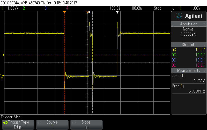
Only in the case of power down, the GPMC control outputs behave strangely.

The power down we have tried once with the Texas board TMDXICE3359,

although the TI board does not contain NAND but relevant are synonymous only the outputs of the processor.

The GPMC control signals are important (see enclosed picture)

- GPMC_CSn0 Chip Select NOR device (measured at resistor R125)

- GPMC_WRn Write Enable (measured on jumper J4)

- WARM RESET RESETIN_OUT (measured at switch S1)


Error Description:

As soon as the supply drops, the PMIC (TPS65910A3) switches the AM335x to the reset.  nPORZ=low -->SYS_WARMRESETn follows the nPORZ. Everything as far as expected.

But what happens then is strange, chip select, write enable and also read enable, push to LOW.

On the basis of the Texas Board TMDXICE3359 interface, the chip select has a 10k pull-up resistor, which can be seen well at the charging curve.

Write eable does not have any outputs actually push pull outputs.

Why do the GPMC Control outputs go low when the reset state is high?

Our problem is that in this case the low level on chip select and write enable on our device leads to an unwanted write access on the NOR device.

Also, a manual override via JTAG Lauterbach, the GPMC Control outputs to GPIO output "push pull high" are configured,

as soon as we perform a cold reset, the outputs go to "LOW" even though the + 3V3 IO supply of the processor is present.


Can you help us here?

8156.tmdxice3359_sch_3h0013_v2_1a.pdf

  • Hi,

    Based on the datasheet Table 4-1. Pin Attributes I would also have expected GPMC_CSn0, GPMC_WEn, and GPMC_OEn_REn to be pulled high during reset, not pushed low then pulled high...
    Its worth noting that after reset these pins are pinmuxed up as GPIOs, and the reset state of the GPIO registers should configure them as inputs, but that is besides the point since the device is clearly still in reset.

    In the scope shot V3_3D is at about 2.3V. GPMC_CSn0, GPMC_WEn, and GPMC_OEn_REn are supplied by VDDSHV1 which is supplied by VAUX2 on the TMDXICE3359 board.
    What does VAUX2 look like when you see observe these signals pushing low?
    When these pins are in reset, I believe they should be weakly pulled high to VDDSHV1. Of course the GPMC_CSn0 also has an external pull to V3_3D, which may explain its faster charge rate.

    However, I cannot yet explain why they drop in voltage right when SYS_WARMRESETn goes low...

    Let me ask internally. Please check on the VAUX2 supply.

    =-=-=-=-
    V6 GPMC_CSn0 @ R125 pull up to V3_3D

    muxmode0 is GPMC_CSn0
    BALL RESET STATE: H
    BALL RESET REL. STATE: H
    RESET REL. MODE [8]: 7
    Muxmode 7: gpio1_29
    ZCZ POWER: VDDSHV1 = VAUX2

    =-=-=-=-
    U6 GPMC_WEn @ J4

    muxmode0 is gpmc_wen
    BALL RESET STATE: H
    BALL RESET REL. STATE: H
    RESET REL. MODE [8]: 7
    Muxmode 7: gpio2_4
    ZCZ POWER: VDDSHV1 = VAUX2

    =-=-=-=-
    T7 GPMC_OEn_REn @ J4
    muxmode0 is gpmc_oen_ren
    BALL RESET STATE: H
    BALL RESET REL. STATE: H
    RESET REL. MODE [8]: 7
    Muxmode 7: gpio2_3
    ZCZ POWER: VDDSHV1 = VAUX2

    =-=-=-=-
    A10 WARMRSTn @ S1
    muxmode0 is nRESETIN_OUT
    BALL RESET STATE: 0
    BALL RESET REL. STATE: 0(PU) (11)
    RESET REL. MODE [8]: 7
    Muxmode 7: gpio2_3
    ZCZ POWER: VDDSHV6 = VAUX2

    (11) The 0(PU) indicates that this terminal is initially low based on the description in the AM335x Technical Reference Manual. However, it is also has a weak internal pullup applied.


    =-=-=-=-=-=-=-=-=-=-=-=-
    Relevant Notes

    6. BALL RESET STATE: State of the terminal while the active low PWRONRSTn terminal is low.
    – 0: The buffer drives VOL (pulldown or pullup resistor not activated)
    0(PD): The buffer drives VOL with an active pulldown resistor
    – 1: The buffer drives VOH (pulldown or pullup resistor not activated)
    1(PU): The buffer drives VOH with an active pullup resistor
    – Z: High-impedance
    – L: High-impedance with an active pulldown resistor
    – H : High-impedance with an active pullup resistor

    7. BALL RESET REL. STATE: State of the terminal after the active low PWRONRSTn terminal transitions from low to high.
    – 0: The buffer drives VOL (pulldown or pullup resistor not activated)
    0(PD): The buffer drives VOL with an active pulldown resistor
    – 1: The buffer drives VOH (pulldown or pullup resistor not activated)
    1(PU): The buffer drives VOH with an active pullup resistor
    – Z: High-impedance.
    – L: High-impedance with an active pulldown resistor
    – H : High-impedance with an active pullup resistor

    8. RESET REL. MODE: The mode is automatically configured after the active low PWRONRSTn terminal transitions from low to high.

    =-=-=-=-=-=-=-
    Checking reset state of GPIO registers in TRM...

    GPIO_OE = FFFFFFFFh after reset
    1h = The corresponding GPIO port is configured as an input.

    GPIO_DATAOUT = 0h after reset - would have output low if output enabled
  • Here answers from customer:

    Q: What about the VAUX2 supply?

    The VAUX2 drops slowly from + 3V3 until the PMIC issues a reset (nPORz) to the processor.

    See picture TMDXICE3359_VAUX3.png

    At the time of WARMRESET, the signals write enable and chip select are then interesting.

    See picture TMDXICE3359_SYS-WARMRESETn.png

    The measurement we have then also made on our design and here, too, the intrusion of the signal is clearly recognizable.

    See the image Target_SYS-WARMRESETn.png

    The question is unfortunately still, what happens in the reset case?

    Why do the GPMC signals go low?

    Here refered scope plots:

    VAUX3:

    SysWarm Reset:

    Target Warm Reset:

  • Hi,

    customer still need answer. Otherwise he has to decide to develop a HW workaround.
  • Hi DJ-NG,

    Were all of these scope shots taken from AM3359ICE board or from the customer board? I am working to acquire an AM3359ICE board to reproduce these waveforms.

    In the VAUX3.png scope shot, the blue waveform is labeled V3-3D (VAUX2). Is that V3_3D (from U32 TPS78633) or VAUX2 (from U22 TPS65910A3)?

    One concern is that on the AM3359ICE board, the GPMC signals from the AM335x device are supplied by VAUX2 (VDDSHV1), but the NOR flash and the pull-up for CSn are supplied by V3_3D. This is not good practice since there can be a current path between different rails. Does the customer board also use two separate rails for the memories and VDDSHV1?
    The issue may be more apparent during power-down, when the capacitance on each rail may differ, leading to different discharge rates. Perhaps the GPMC control signals are going low because the IO buffers supplied by VAUX2 have collapsed as VUX2 discharges... The signals could then be pulled towards V3_3D... This makes sense at least for CSn because it has an external pull-up to V3_3D. It does not, however, explain why WEn appears to recharge after reset since there is no pull-up on WEn (on the AM3359ICE board) and it is an input to the memory... Both CSn and WEn appear to slowly charge up after reset. It might be telling to observe these signals longer after reset (and with V3_3D and VAUX2 probed) to see what rail the GPMC signals are being pulled to. We could also experiment by blue-wiring the memory supply and chip select pull-up to VAUX2 instead of V3_3D to see if that changes this observed behavior at reset.

    We are also interested in seeing PORz in relation to SYS-WARMRESETn. Can you confirm that all of your scope shots show WARMRESETn? This signal should go low shortly after PORz goes low.

    There have been instances with other peripherals where an unexpected race condition occurs between reset (from PORz) arriving at a peripheral before the pinmux and rest of system. The pin might go to a different state after just a peripheral reset when compared to a full system reset. The takeaway is that the reset states provided in the data sheet may only apply during power-up and cannot be guaranteed during power-down... We should be able to reproduce that scenario by applying a local reset only to the GPMC peripheral by writing a '1' to the SOFTRESET of the GPMC_SYSCONFIG register. If this is the case, then we could also monitor any CSn except for CSn0 during reset. After reset only CSn0 is active. See GPMC_CONFIG7_0 CSVALID bit: Chip-select enable (reset value is 1 for CS[0] (active low) and 0 for CS[1] to CS[5] (active low)).

    Let me first locate an AM3359ICE board and try to reproduce some of these signals. Please try to find answers to my questions in parallel.

    Regards,
    Mark

  • Hi Mark,

    here answers:

    - Two scopes, named TMDXICE3359*.png have been take from AM3359ICE board. The scope TARGET*.png was of course taken from our own board.

    - The blue waveform labled V3-3D(VAUX2) is V3-3D from U32 TPS78633

    - The customer uses a single 3V3 rail for all 3V3 related components

    - Warmreset behavior is shown on TMDXICE3359*.png. As the customer uses mainly nPORZ for system reset an nWarmreset as reset path for connected components the TARGET*.png shows nPORZ
  • HI DJ-NG,

    Thanks for the answers. It is good that the customer uses a single rail for memory and processor (unlike the ICE board).

    Digging into the theory that the PORz reset signal has different paths to the pinmux logic and to the GPMC peripheral, I simulated the case where reset arrives at the GPMC peripheral before the pinmux logic by applying a local software reset to the GPMC peripheral.

    I was able to capture CSn driving low after applying a soft reset through the SOFTRESET bit of the GPMC_SYSCONFIG register. See scope shot below.

    I think CSn0 could drive low during the local soft reset (or maybe after releasing the reset) because the reset state of the GPMC registers activates GPMC_CSn0 at GPMC_FCLK cycle 0. I would like to see what happens with the other CSn signals (not CSn0) since they do not get activated at reset.

    The description for the CSVALID bit in the GPMC_CONFIG7_0 register states that the Chip-select enable reset value is 1 for CS[0]. And 1h = CS (active low) enabled.

    CSONTIME, CSRDOFFTIME, and  CSWROFFTIME all reset to 0h in the GPMC_CONFIG2_0 register so the CSn0 should go low at FCLK cycle 0, but it should also go high at FCLK cycle 0... I'm not sure yet how the IP reacts if ONTIME = OFFTIME.

    We also think it might be plausible to experience some uncertainty on the pins as the reset signal propagates through the pinmux logic. It uses asynchronous logic that might go through unexpected intermediate states as the pinmux registers transition to their reset states.

    It may be justly prudent for the customer to implement some external isolation between the processor and the memories that kicks in when the first rail begins going down (without back-powering any non-failsafe IOs during power down). This could be tricky, but is intended to prevent unwanted signals from corrupting the memory.

    I'll let you know if I find out more regarding the GPMC signals driving low at reset.

    Regards,
    Mark