This thread has been locked.

If you have a related question, please click the "Ask a related question" button in the top right corner. The newly created question will be automatically linked to this question.

TDA3: tda3x_chqspi_clock64mhz.bin

Part Number: TDA3

Hello.

I'm trying to compare 'sbl.chimage' over 'sbl.tiimage'.

I can't see any speed advantage for the chimage-version while booting from qspi-flash (TDA3XXEVM).

The chimage-header is correct?

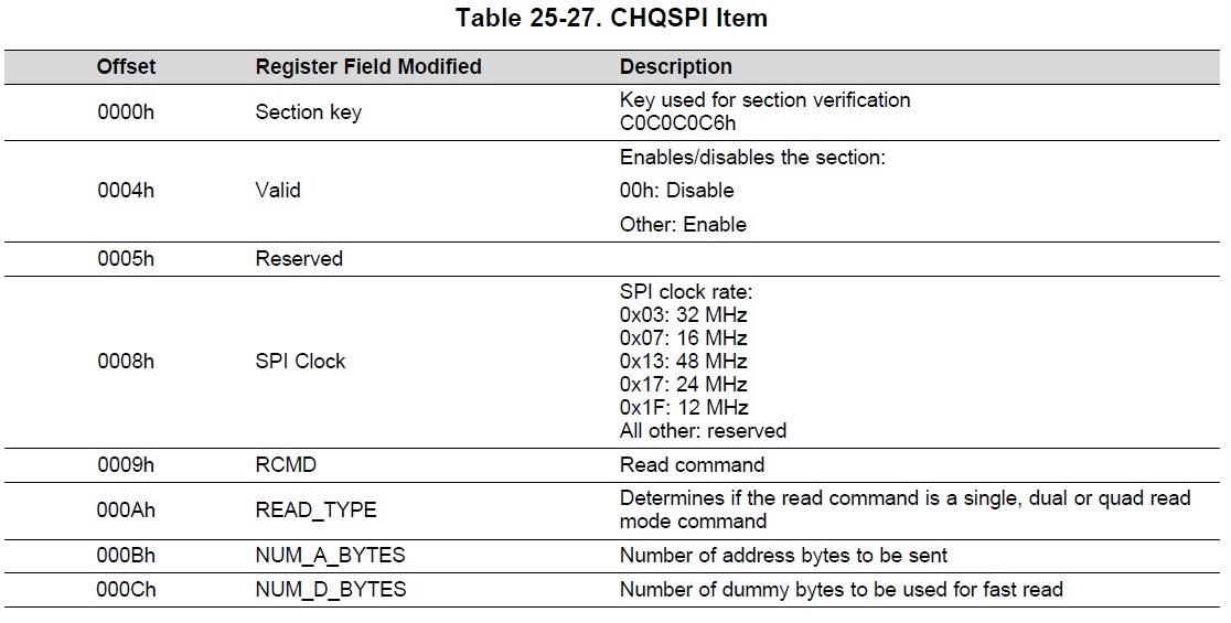
Here is Table 25-27 from TRM.

But, here is content of
'ti_components/drivers/pdk_01_07_00_16/packages/ti/boot/sbl_auto/tools/chimage/tda3x_chqspi_clock64mhz.bin'

Here is result:
0x040 (0x00) Section key : "C0 C0 C0 C6" = OK
0x044 (0x04) Valid       : "00"          = (disable) ???
0x045 (0x05) Reserved    : "00"
0x046-0x047              : "00 01"       = (unknown fields) !!
0x048 (0x08) SPI Clock   : "00"          = (All other: Reserved) ???
0x049 (0x09) RCMD        : "00"          = ?
0x04A (0x0A) READ_TYPE   : "FF"          = ?
0x04B (0x0B) NUM_A_BYTES : "01"          = ?
0x04C (0x0C) NUM_D_BYTES : "00"          = ?
0x04D-0x04F              : "00 FF 00"    = (unknown fields) !!

Why 'valid' is disabled? Where are 64Mhz speed selection? Could you explain RCMD,READ_TYPE,NUM_A_BYTES and NUM_D_BYTES fields? Does the file name (offs:0x014-0x01F) have any meaning?

Thank you in advance.

PS: Vision SDK is 3.0.0.0

  • Hi Senchuss,

    CH bin is in Little Endian format so you need to decipher it such that the 8 LSBs represent 0x0 and 8 MSBs repesent 0x3

    Hence the CH can be read as given below:
    0x00 Section key : "C0 C0 C0 C6" = Matches TRM
    0x04 Valid : "01" = Valid
    0x05-0x7 : "00 00 00" = Reserved
    0x08 SPI Clock : "01" = 64 MHz (This needs to be documented in TRM).
    0x09 RCMD : "ff" = When value read at 0x9 is FF, RBL does not update RCMD, READ_TYPE, NUM_A_BYTES and NUM_D_BYTES.

    There are two input clocks to SPI: 128 MHz and 192 MHz. The first nibble represents the mux select: 0x0 selects 128 MHz and 0x1 selects 192 MHz.
    Second nibble refers to divider. Clock gets divided by (divider + 1).
    Hence 0x01 means SPI clock is (128/1+1)= 64 MHz.
    I will file a bug on TRM in order to update the table for 0x01 value

    Regards,
    Rishabh
  • Hi Senchuss,

    CH will lead to improvement in time taken by RBL to load SBL.
    SBL has a print that says "Reset to SBL Init Cycles".
    Can you check it and verify if you see any difference.
    Thanks

    Regards,
    Rishabh
  • Hi Rishabh. Thank you very much! The picture was updated according to your words.

  • Thank you! Yes. I see 1ms advantage.

    sbl_qspi_opp_high_ipu1_0_release.tiimage

    Reset to SBL Init Cycles - 365  (11.13 ms)

    sbl_qspi_opp_high_ipu1_0_release.chimage

    Reset to SBL Init Cycles - 331  (10.10 ms)

  • Hi Senchuss,

    Thanks for the confirmation.

    Regards,
    Rishabh
  • Hi, Rishabh. Let me ask one more question.
    How does the OPP affect SBL-booting speed?
    I can see that SBL with OPP=NOM is faster then OPP=HIGH. It seems strange.
    Here are my results.

  • Hi Senchuss,

    AVS 0 takes more time for OPP High and OD as compared to NOM.
    The default voltage set at the voltage rails is quite close to OPP NOM voltage. So the time taken for voltage ramp is lesser in case of OPP NOM.
    AVS 0 time is accounted in SBL initial config cycles and hence you see the difference.

    Kindly open a new thread for any new questions as the original question was about CHQSPI and not the SBL boot time.
    Thanks.

    Regards,
    Rishabh