This thread has been locked.

If you have a related question, please click the "Ask a related question" button in the top right corner. The newly created question will be automatically linked to this question.

CPU not ready to connect after accessing the USB

Other Parts Discussed in Thread: OMAP-L138

Hi all,

I have a customer that is having problems to connect to CCS in his custom board (but not in the EVM), he is getting this error (clicking "yes" did not solve it):

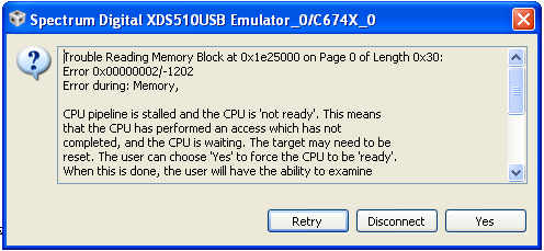
We analyzed the problem and it does not seem to be a CCS issue as he did not make any updates and the same software and same GEL file work fine in the EVM.

When the problem started occurring, no hardware changes were made. The problem occurred the first time he tried to access the USB1 peripheral module. No initialization changes were made. Error occurs even before any software is sent to the board. No upgrades in CCS have been made in a while.

Both devices are: XOMAPL137ZKB3 or:Experimental OmapL137 SiliconRev1.0 0-90*C 256BGA 300MHZ

I asked to make sure that the board was in EMU boot and he did, but no change.

Could it be related to some USB state? Is there more information on SPRZ291D: Advisory 1.1.9 (Slew rate on USB0 and USB1 power supplies)?

  • Mariana,

    Is it possible that USB0 is also enabled with USB1?  I see some "multiple interrupt" type of advisories attached to USB0 that may be keeping the DSP busy.  Is there any other activity going on in the background?  Some of the DSP cache issues can create a system deadlock.

    -Tommy

  • Hi Tommy,

    I will ask the customer to take a look at your answer.


  • oops. 

  • Mariana

     I am assuming USB1 clocks are enabled via PSC , and also if there is any dependency for USB0 as the clock source for USB1, then USB0 is enabled (Chapter on Device clocking in the System guide highlight the various clock combinations for USB1 and USB0.

    Finally, I hope the customer hardware has the correct hook up for USB power and ground pins? Is a schematic check required?

    Regards

    Mukul

  • I am the customer that Mariana is speaking of, and:
    1. The USB0 is accessible through CCSv4 while USB1 is not. With the exact same GEL File (and like wise PSC settings) I can access both on the EVM.
    2. The pins F3 and H4 had no effect on this problem. (we were able to connect and disconnect these on the custom board) 

  • Are H5, E3, C1 and C2 all connected to 3.3V and 1.8V supplies ?


  • I have seen this error before when the OHCI controller is enabled through the low power / sleep controller, but the 48MHz USB reference clock is not running.

    The registers inside the OHCI controller are actually mostly clocked from the 48MHz clock, and you can't access them when this clock isn't running.  The access will

    start but timeout with an error - resulting in the CCS error.

    I would look at  Lit # SPRUFM8 section 2.1.3 for a description of how to get a 48MHz clock to the OHCI controller.
    But in a nutshell - either it comes in on a pin or you can get it from the USB0 High-Speed PHY PLL.  

    It is quite possible that the USB0 peripheral memory mapped registers are accessible while the USB0 Phy isn't setup to provide a 48MHz clock to the USB1 host.

    I would check the register CFGCHIP2 which you can find documented in section 11.5.16 of Lit# SPRUGM7 OMAP-L138 Applications Processor System Reference Guide.

    This register contains the control bits for the USB0 phy as well as the selection of whether or not the USB1 module uses the 48MHz reference from a pin or from the USB0 phy.

  • I am trying to use the internal clock. And even after setting Cfgchip2 to this:
     CFGChip2

    As you can see, USB0REF_FREQ = 2; USB0PHYCLKMUX = 1; USB1PHYCLKMUX = 1;

    As a note, it appears that the EVM may be getting an external clock. Can anyone confirm this?

  • We just confirmed, the B5 pin (USBREFCLKIN) on the EVM has 24.576MHz present.

    This is being sourced from U39, McASP Clock.

    I can't imagine this is correct...

  • Jonathan
    It looks to be correct,  there is a 0 ohm resistor connecting the T_AIC_MCLK -AHCLKX1 to USBREFCLKIN. Also in the Spectrum Digital Gel file I see the following

    hotmenu
    Setup_System_Config( )
    {

    GEL_TextOut( "Setup PINMUX Registers... " );
    KICK0R = 0x83e70b13; // Kick0 register + data (unlock)
    KICK1R = 0x95a4f1e0; // Kick1 register + data (unlock)

    PINMUX0 = 0x11112188; // EMIFB, Check EMU0/RTCK
    PINMUX1 = 0x11111111; // EMIFB
    PINMUX2 = 0x11111111; // EMIFB
    PINMUX3 = 0x11111111; // EMIFB
    PINMUX4 = 0x11111111; // EMIFB
    PINMUX5 = 0x11111111; // EMIFB
    PINMUX6 = 0x11111111; // EMIFB
    PINMUX7 = 0x11111111; // EMIFB, SPI0
    PINMUX8 = 0x21122111; // UART2, McASP1, I2C0, I2C1
    PINMUX9 = 0x11011112; // RMII CLK, McASP0, USB_DRVVBUS, UART2
    PINMUX10 = 0x22222221; // RMII/ McASP0
    PINMUX11 = 0x11142222; // McASP1, UART1, McASP0, MDIO (last 2 digits 0x22 for MDIO instead of GPIO)
    PINMUX12 = 0x11111111; // McASP0 / McASP1
    PINMUX13 = 0x22111111; // SD / McASP1
    PINMUX14 = 0x88222222; // SD / EMIFA
    PINMUX15 = 0x21888888; // SD / EMIFA
    PINMUX16 = 0x11111112; // SD / EMIFA
    PINMUX17 = 0x00100111; // EMIFA
    PINMUX18 = 0x11111111; // EMIFA
    PINMUX19 = 0x00000001; // EMIFA

    CFGCHIP2 |= 0x00001000; // Enable USB1 clock

    GEL_TextOut( "[Done]\n" );
    }\

    Setting bit CFGCHIP2 bit 12 to 1.


  • Hi Jonathan,

    Do you have another custom board to test? Does the problem happen in only one of your custom boards in case you have more than one?

  • All of the custom boards have the same problem. And the EVM stops working once the resistor that is feeding B5 is lifted.

  • I quickly tried to comment out the line that highlighted in the GEL file and try to access the USB1 memory map on the SD OMAPL137 EVM and I get exactly the same emulation error as was posted in the first post. So it does look like a clock source issue.

    Regards

    Mukul

  • From PLL Controller all the way to the USB1PHYCLKMUX, what registers must be enabled to pass the clock from the 24MHz crystal (pins F1, F2) to the USB1 module.

  • I don't have the EVM schematics, but 24.576MHz is the master clock frequency required for DVD audio (48KHz sample rate).

    So, I think the board has probably been designed such that 24.576MHz is supposed to feed the McASP, and the USB1 should use the internal USB0 PLL.

    The other thing to check is that the USB0 PHY has power, because the PLL in the PHY wouldn't be able to produce a clock without power.

  • With bit 12 of CFGChip2 set (as in Mukul's posts) that very same 24.576MHz clock is what is feeding the USB1 module, albeit at an incorrect rate. It just happens that that is rapid enough to not cause errors when reading registers.

  • The clocking details for USB0/USB1 are in the OMAPL137 System Guide

    http://focus.ti.com/lit/ug/sprug84c/sprug84c.pdf

    (Table 7-4). I would expect what you want to use is third row settings? Without looking at your custom hardware schematics, and so far from the posts provided, check list would be

    1) Power Applied to USB0 and USB1 power pins

    2) Clock enabled via PSC for both USB0 and USB1

    3) CFGCHIP2 setup correctly to have USB0 source clock to USB1 and likely USB0 from AUXCLK. I can't try this anywhere , but give a value of CFGCHIP2= 0x9F2 and see if this works.

    This should likely be all that you need to have your CPU accesses to USB1 MMR space work.

    Regards

    Mukul

  • 1) Power is applied to the pins

    2) PSC1.MDSTAT1.State = 3 PSC1.MDSTAT2.State = 3

    3)Sys_Cfg_Regs.CFGChip2.all must be set to a minimum of 0x8C2 (0x9F2 also works).

    To prevent processor lockups:

    Sys_Cfg_Regs.CFGChip2.USB0Ref_Freq must be set (read only bit) before reading from USB_1.


    Mukul your CFGChip2 was the key.

  • One mistake in the last post:


    1) Power is applied to the pins

    2) PSC1.MDSTAT1.State = 3 PSC1.MDSTAT2.State = 3

    3)Sys_Cfg_Regs.CFGChip2.all must be set to a minimum of 0x8C2 (0x9F2 also works).

    To prevent processor lockups:

    Sys_Cfg_Regs.CFGChip2.USB0PHYCLKGD must be set (read only bit) before reading from USB_1.


    Mukul your CFGChip2 was the key.