This thread has been locked.

If you have a related question, please click the "Ask a related question" button in the top right corner. The newly created question will be automatically linked to this question.

RTOS/TMS320C6678: PCIe Root Complex configuration / examples

Part Number: TMS320C6678

Tool/software: TI-RTOS

Hello,

We've designed a system similar to C6678 EVM where the C6678 DSP is connected to Virtex 7 FPGA via the PCIe Gen2 x2. The DSP planned to be the Root Complex side.

The needed steps to do to verify the PCIe connection are reading:

  • Vendor/Sub-system Vendor ID
  • Device/Sub-system Device ID
  • Class code
  • Register offsets within Bar 0

The first 3 steps we've already succeeded to do but the 4th one is still the open side.

The only example I found was in ~/ti/pdk_c667x_2_0_7/packages/ti/drv/pcie/example/sample/src/pcie_sample.c path and I couldn't figure out how I can modify it to read the BAR0 space registers (from FPGA side the BAR0 size is configured 64KB) instead of pre-defined outbound address space (started from 0x70000000) and inbound address space (started from 0x90000000).

Could you please advice how to find the needed examples / modify the sources for it?

Regards

Andranik

  • Hi Andranik,

    I've forwarded your query to the software experts. Their feedback should be posted here.

    BR
    Tsvetolin Shulev
  • Hi!

    There is excellent memo about PCIe addressing www.ti.com/.../sprabk8.pdf.

    Before you could read anything from FPGA you have to configure its BARs. Confusing point is that all TI examples are written for the case, where processor exist on both RC and EP, and those processors do configure their local BARs. With that will not work. Instead, you have to configure remote EP, that is FPGA's BAR(s). That looks pretty similar to configuring DSP's own BARs with the only exception, that BAR location is remote, like follows:

    pcieRet_e      retval;
    pcieBarCfg_t   barCfg;
    
    /* Configure BARs */
    /* BAR0 for APllication registers & BRAMs in FPGA fabric */
    barCfg.location = pcie_LOCATION_REMOTE;
    barCfg.mode     = pcie_EP_MODE;
    barCfg.base     = FPGA_BAR0_BASE;
    barCfg.prefetch = pcie_BAR_NON_PREF;
    barCfg.type     = pcie_BAR_TYPE32;
    barCfg.memSpace = pcie_BAR_MEM_MEM;
    barCfg.idx      = 0;
    
    if ( pcie_RET_OK != ( retval = Pcie_cfgBar(handle, &barCfg) ) )
    ...
    

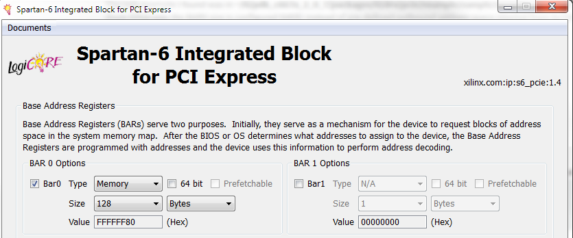
    This should be familiar to you, the only question how to define FPGA_BAR0_BASE. One may think, that BAR is defined by two registers, namely base address and base mask. The latter is set implicitly when you define requested address range. When you were setting your FPGA's PCIe IP core there was a step to define BAR size. Somewhere below there was a window with calculated mask. Image below is for much older device and toolchain, yours might look different, but concept is the same:

    As you see, for 128 bytes one needs 7 address bits, and those 7 LSbs are zeroed in mask. Instead, all upper bits with ones can define base itself. For your case, when you are requesting 64KB, the mask will look like 0xFFFF_0000.

    Now you may think, that every incoming TLP is matched against target BARs. Address field from the packet is ANDed with BAR mask and the result is compared against BAR address. If they match, that BAR was hit and the packet gets accepted on that BAR. See the example:

    Mask 0xFFFF_FF00 for 256B window
    Configure BAR to 0x0000_0200 (write 0x0000_0200):
      0xFFFF_FF00
     &0x0000_0200 
    = 0x0000_0200
    
    Access example:
    	PCIe address 0x0000_0224
                     &0xFFFF_FF00
                      0x0000_0200 compare to BAR
                 BAR: 0x0000_0200 --> BAR hit
    
    	PCIe address 0x0000_1024
                     &0xFFFF_FF00
                      0x0000_1000 compare to BAR
                 BAR: 0x0000_0200 --> BAR not hit


    You mentioned, you are using outbound address translation with destination of 0x70000000. That means, access to PCIe address window (0x6000_0000) gets translated to 0x7000_0000 range and your TLP will reach your FPGA with 0x7000_0000 based address field. Thus, you have to configure BAR with 0x7000_0000 based base address. Imagine, you want to put your BAR0 at the very origin, then write 0x7000_0000 to BAR0 with Pcie_cfgBar() call. Imagine, you'd like to define another 64KB window as BAR1 just next to BAR0, then write 0x7001_0000 to BAR1 and every access to 0x6001_XXXX will land to BAR1.

    Hope this helps.

  • Thanks rrlagic for the detailed experience on setting FPGA!

    Andranik, is the suggestion helpful? Is the issue resolved?

    Regards, Eric
  • Thank you for complete procedure description - we've finally tested the FPGA to DSP x2 PCIe connection and were able to read the needed BAR0 registers.

    Thanks again for efforts.

    Regards

    Andranik