This thread has been locked.

If you have a related question, please click the "Ask a related question" button in the top right corner. The newly created question will be automatically linked to this question.

Linux/DRA744: DRA744: HOW TO Display 2880x960 resolution by using extended display features and 2 VOUT

Part Number: DRA744

Tool/software: Linux

We are using the DRA7xx infotainment processor J6 and the linux kernel 4.4.23.

In addition to the e2e post:

https://e2e.ti.com/support/arm/automotive_processors/f/1020/p/575710/2259260#2259260

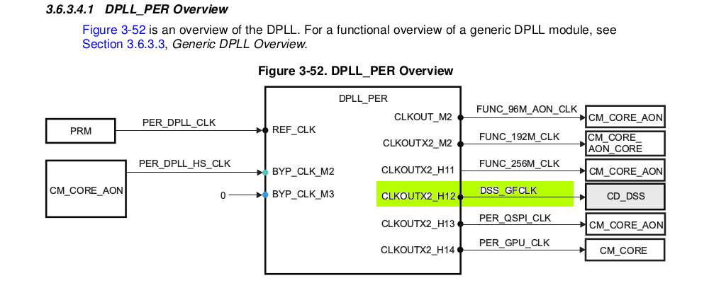
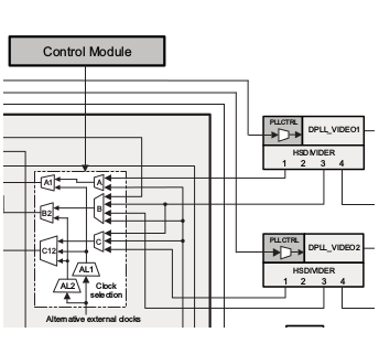
and with reference to the figure: Figure 11-4. Display Subsystem Clock Tree, see figure below.

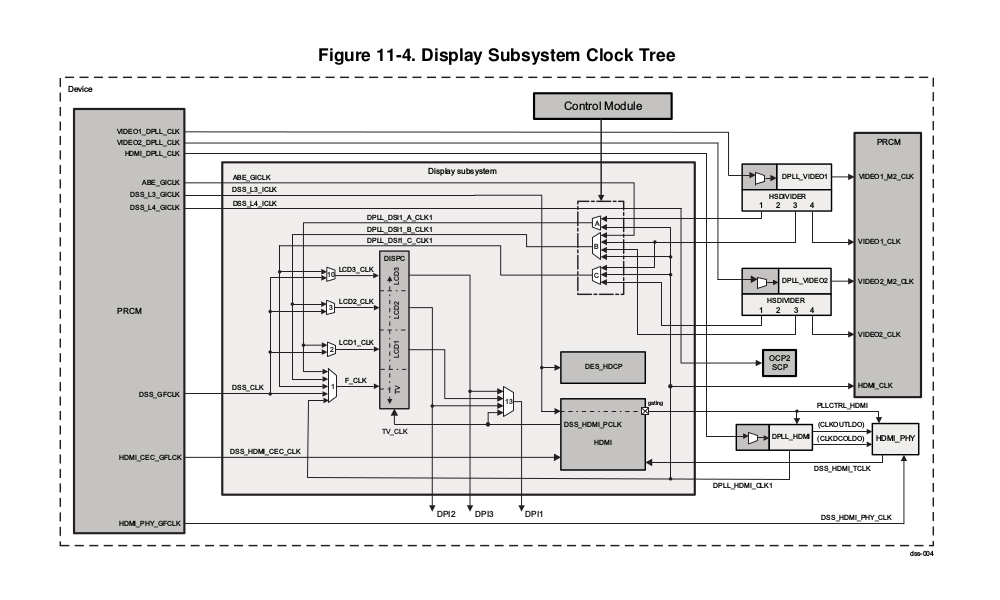
By default the hdmi driver (in the drivers/gpu/drm/omapdrm) is working with this configuration:

F_CLK (multiplexer 1) is sourced from DSS_CLK (DSS_CLK_SRC_FCK)

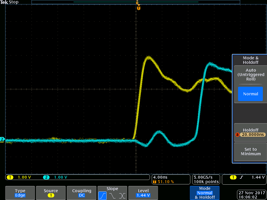
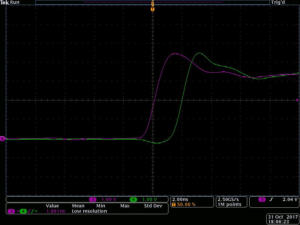
If we try to synchronize the LCDs using the common DSS_CLK source (instead of the Video PLL lines from DPLLs) and introducing a 'warmreset' before enabling the displays, the time between the 2 Vout HSYNC is ~2ns (see scope figure below).

But with this method the HDMI is no more working.

It is possible to configure the HDMI to use an internal generated clock instead of the default DSS_CLK?

How it is possible?

  • This is the standard configuration that uses LCD1 and LCD2 with PLL Video1 and PLL Video 2 active (dss_clockdump):

    /* standard configuration */
    
    -bash-3.2# ./dss_clockdumps.sh 
    
    
    =====================DSS clock script===================
    Dumps internal clocks and muxes of DSS
    
    CTRL_CORE_DSS_PLL_CONTROL (0x4a002538) = 0x000002A0
    video1 PLL :  Enabled
    video2 PLL :  Enabled
    HDMI   PLL :  Enabled
    DSI1_A_CLK mux : DPLL Video1
    DSI1_B_CLK mux : DPLL video2
    DSI1_C_CLK mux : DPLL Video1
    
    DSS_CTRL (0x58000040) = 0x00011001
     2: LCD1 clk switch :  DSI1_A_CLK
     3: LCD2 clk switch :  DSI1_B_CLK
    10: LCD3 clk switch :  DSS clk
     1: func clk switch :  DSS clk
    13: DPI1 output     :  LCD1
    
    DSS_STATUS (0x5800005C) = 0x01409282
    
    DSI_CLK_CTRL (0x58004054) = 0x80004001
    
    CM_DSS_CLKSTCTRL (0x4A009100) = 0x00041F03
    
    CM_DSS_DSS_CLKCTRL (0x4A009120) = 0x00003702
    
    ========================================================
    Register dump for DPLL video1
    |----------------------------|
    | Address (hex) | Data (hex) |
    |----------------------------|
    | 0x58004300    | 0x00000018 |
    | 0x58004304    | 0x00002283 |
    | 0x58004308    | 0x00000000 |
    | 0x5800430C    | 0x012AD44E |
    | 0x58004310    | 0x00616008 |
    | 0x58004314    | 0x00000000 |
    | 0x58004318    | 0x00000000 |
    | 0x5800431C    | 0x00000000 |
    | 0x58004320    | 0x00000000 |
    |----------------------------|
    Details for DPLL video1
    PLL status  :  Locked
    M4 hsdiv(1) :  Active
    M5 hsdiv(2) :  inactive
    M6 hsdiv(3) :  inactive
    M7 hsdiv(4) :  inactive
    
    PLL_REGM   =  1386
    PLL_REGN   =  39
    M4 DIV     =  9
    M6 DIV     =  0
    M7 DIV     =  0
    
    Clock calculations (DPLL video1)
    sysclk = 20000000
    DCO clk = sysclk * 2 * REGM / (REGN + 1) = 1386000000
    M4clk (clkcout1) = DCO clk / (M4 DIV + 1) = 138600000
    M6clk (clkcout3) = DCO clk / (M6 DIV + 1) = 0
    M7clk (clkcout4) = DCO clk / (M7 DIV + 1) = 0
    
    ========================================================
    Register dump for DPLL video2
    |----------------------------|
    | Address (hex) | Data (hex) |
    |----------------------------|
    | 0x58009300    | 0x00000018 |
    | 0x58009304    | 0x00002603 |
    | 0x58009308    | 0x00000000 |
    | 0x5800930C    | 0x000DCE4E |
    | 0x58009310    | 0x00E06008 |
    | 0x58009314    | 0x0000001E |
    | 0x58009318    | 0x00000000 |
    | 0x5800931C    | 0x00000000 |
    | 0x58009320    | 0x00000000 |
    |----------------------------|
    Details for DPLL video2
    PLL status  :  Locked
    M4 hsdiv(1) :  inactive
    M5 hsdiv(2) :  inactive
    M6 hsdiv(3) :  Active
    M7 hsdiv(4) :  inactive
    
    PLL_REGM   =  1767
    PLL_REGN   =  39
    M4 DIV     =  0
    M6 DIV     =  30
    M7 DIV     =  0
    
    Clock calculations (DPLL video2)
    sysclk = 20000000
    DCO clk = sysclk * 2 * REGM / (REGN + 1) = 1767000000
    M4clk (clkcout1) = DCO clk / (M4 DIV + 1) = 0
    M6clk (clkcout3) = DCO clk / (M6 DIV + 1) = 57000000
    M7clk (clkcout4) = DCO clk / (M7 DIV + 1) = 0
    
    ========================================================
    Register dump for DPLL hdmi
    |----------------------------|
    | Address (hex) | Data (hex) |
    |----------------------------|
    | 0x58040200    | 0x00000018 |
    | 0x58040204    | 0x00000003 |
    | 0x58040208    | 0x00000000 |
    | 0x5804020C    | 0x00030A0E |
    | 0x58040210    | 0x00602004 |
    | 0x58040214    | 0x00001000 |
    | 0x58040218    | 0x00000000 |
    | 0x5804021C    | 0x00000000 |
    | 0x58040220    | 0x00058106 |
    |----------------------------|
    Details for DPLL hdmi
    PLL status  :  Locked
    M4 hsdiv(1) :  inactive
    M5 hsdiv(2) :  inactive
    M6 hsdiv(3) :  inactive
    M7 hsdiv(4) :  inactive
    
    PLL_REGM   =  389
    PLL_REGN   =  7
    M4 DIV     =  0
    M6 DIV     =  0
    M7 DIV     =  0
    PLL_REGM2  =  1
    PLL_REGM_F =  1
    PLL_SD  =  4
    HDMI_SSC_CONFIGURATION1(should be zero) 0x00000000
    HDMI_SSC_CONFIGURATION2(should be zero) 0x00000000
    
    Clock calculations (DPLL hdmi)
    sysclk = 20000000
    CLKOUT = sysclk * REGM / (REGM2 * (REGN + 1)) = 972500000
    
    ========================================================
    Clock O/P of MUXes
    DPLL PER H12 Output 192000000
    CM_DIV_H12_DPLL_PER (0x4A00815C) = 0x00000204
    
    DSI1_A_CLK :  138600000
    DSI1_B_CLK :  57000000
    DSI1_C_CLK :  0
    
    DISPC_DIVISOR (0x58001804) = 0x00010001
    
     2: LCD1 clk :  138600000
     3: LCD2 clk :  57000000
    10: LCD3 clk :  192000000
     1: func clk :  192000000
    
    LCD1 logic clk(/ 1 ) :  138600000  pix clk(/ 2 ) :  69300000
    LCD2 logic clk(/ 1 ) :  57000000  pix clk(/ 2 ) :  28500000
    LCD3 logic clk(/ 4 ) :  48000000  pix clk(/ 1 ) :  48000000
    

  • To obtain the synchronization between the HSYNC (2ns delay as in the figure above) we used the DSS_CLK as F_CLK source, common to LCD1 and LCD2 and we disabled the Video PLLs:

    /* our configuration - DPLL Video inactive */
    
    -bash-3.2# ./dss_clockdumps.sh 
    
    
    =====================DSS clock script===================
    Dumps internal clocks and muxes of DSS
    
    CTRL_CORE_DSS_PLL_CONTROL (0x4a002538) = 0x000002AB
    video1 PLL :  Disabled
    video2 PLL :  Disabled
    HDMI   PLL :  Enabled
    DSI1_A_CLK mux : DPLL HDMI
    DSI1_B_CLK mux : DPLL video2
    DSI1_C_CLK mux : DPLL Video1
    
    DSS_CTRL (0x58000040) = 0x00010000
     2: LCD1 clk switch :  DSS clk
     3: LCD2 clk switch :  DSS clk
    10: LCD3 clk switch :  DSS clk
     1: func clk switch :  DSS clk
    13: DPI1 output     :  LCD1
    
    DSS_STATUS (0x5800005C) = 0x01408A81
    
    DSI_CLK_CTRL (0x58004054) = 0x00000001
    
    CM_DSS_CLKSTCTRL (0x4A009100) = 0x00040B03
    
    CM_DSS_DSS_CLKCTRL (0x4A009120) = 0x00000702
    
    ========================================================
    Register dump for DPLL hdmi
    |----------------------------|
    | Address (hex) | Data (hex) |
    |----------------------------|
    | 0x58040200    | 0x00000018 |
    | 0x58040204    | 0x00000003 |
    | 0x58040208    | 0x00000000 |
    | 0x5804020C    | 0x00030A0E |
    | 0x58040210    | 0x00602004 |
    | 0x58040214    | 0x00001000 |
    | 0x58040218    | 0x00000000 |
    | 0x5804021C    | 0x00000000 |
    | 0x58040220    | 0x00058106 |
    |----------------------------|
    Details for DPLL hdmi
    PLL status  :  Locked
    M4 hsdiv(1) :  inactive
    M5 hsdiv(2) :  inactive
    M6 hsdiv(3) :  inactive
    M7 hsdiv(4) :  inactive
    
    PLL_REGM   =  389
    PLL_REGN   =  7
    M4 DIV     =  0
    M6 DIV     =  0
    M7 DIV     =  0
    PLL_REGM2  =  1
    PLL_REGM_F =  1
    PLL_SD  =  4
    HDMI_SSC_CONFIGURATION1(should be zero) 0x00000000
    HDMI_SSC_CONFIGURATION2(should be zero) 0x00000000
    
    Clock calculations (DPLL hdmi)
    sysclk = 20000000
    CLKOUT = sysclk * REGM / (REGM2 * (REGN + 1)) = 972500000
    
    ========================================================
    Clock O/P of MUXes
    DPLL PER H12 Output 69000000
    CM_DIV_H12_DPLL_PER (0x4A00815C) = 0x0000020B
    
    DSI1_A_CLK :  972500000
    DSI1_B_CLK :  0
    DSI1_C_CLK :  0
    
    DISPC_DIVISOR (0x58001804) = 0x00010001
    
     2: LCD1 clk :  69000000
     3: LCD2 clk :  69000000
    10: LCD3 clk :  69000000
     1: func clk :  69000000
    
    LCD1 logic clk(/ 1 ) :  69000000  pix clk(/ 1 ) :  69000000
    LCD2 logic clk(/ 1 ) :  69000000  pix clk(/ 1 ) :  69000000
    LCD3 logic clk(/ 4 ) :  17250000  pix clk(/ 1 ) :  17250000
    

  • Hi Massimo,

    I have forwarded your question to DSS expert.

    Regards,
    Yordan
  • Hi Massimo,

    I need a couple of days to get back to you on this question. I need to understand why HDMI would stop functioning.

    regards,
    Venkat
  • Hi Venkat, thank you.

    I add more details.

    To made the LCDs working with the common DSS_CLK, we modified, in the driver dpi.c, the function that select the clock source for the dra7xx:

    diff --git a/drivers/gpu/drm/omapdrm/dss/dpi.c b/drivers/gpu/drm/omapdrm/dss/dpi.c
    index 03429c6..272d73f 100644
    --- a/drivers/gpu/drm/omapdrm/dss/dpi.c
    +++ b/drivers/gpu/drm/omapdrm/dss/dpi.c
    @@ -78,24 +78,24 @@ static enum dss_clk_source dpi_get_clk_src_dra7xx(enum omap_channel channel)
    switch (channel) {
    case OMAP_DSS_CHANNEL_LCD:
    {
    + if(dss_pll_find_by_src(DSS_CLK_SRC_FCK) == NULL)
    + return DSS_CLK_SRC_FCK;
    if (dss_pll_find_by_src(DSS_CLK_SRC_PLL1_1))
    return DSS_CLK_SRC_PLL1_1;
    }
    case OMAP_DSS_CHANNEL_LCD2:
    {
    + if(dss_pll_find_by_src(DSS_CLK_SRC_FCK) == NULL)
    + return DSS_CLK_SRC_FCK;
    if (dss_pll_find_by_src(DSS_CLK_SRC_PLL1_3))
    return DSS_CLK_SRC_PLL1_3;
    + if (dss_pll_find_by_src(DSS_CLK_SRC_PLL2_3))
    + return DSS_CLK_SRC_PLL2_3;
    }
    case OMAP_DSS_CHANNEL_LCD3:
    {
    + if(dss_pll_find_by_src(DSS_CLK_SRC_FCK) == NULL)
    + return DSS_CLK_SRC_FCK;
    if (dss_pll_find_by_src(DSS_CLK_SRC_PLL2_1))
    return DSS_CLK_SRC_PLL2_1;
    if (dss_pll_find_by_src(DSS_CLK_SRC_PLL1_3))
     
      
    In this way (and adding a warmreset before the LCDs enable) we obtain the LCDs working in synchronization with the 2ns delay.
    In the driver we see the DSS_CLK is used to create the F_CLK signal for the dispc.
     
    One difference applying this patch is in the H12 divisor register: CM_DIV_H12_DPLL_PER
    that passes from 0x00000204 to 0x0000020B (change of the DPLL (H12+1) post-divider factor from 4 to B).
     
    If we force this register to the old value manually,
    devmem2 0x4a00815c 0x00000204
    we obtain that HDMI works but the LCDs doesn't.
     
    We would like to be sure that this divisor, CM_DIV_H12_DPLL_PER, has influence only on the DSS subsystem or know if this clock signal is important also for other peripherals, different from DSS. This is another important question for us.
     
     
    Thank you very much.
  • Hi,

    Sorry for the delay in response.

    DPLL_PER HSDIV 12 is only fed into the DSS_GFCLK. This does impact any other IP.

    What are the pixel clock frequencies that you are trying to achieve for the LCD output and for the HDMI?

    Instead of using the DSS functional clock, have you considered using the DPLL Video1 HS DIV3 as input to LCD2 and LCD3? LCD3 can be output to LCD1 output if desired using the parallel_sel mux inside DSS?

    regards,
    Venkat
  • Thank you for your response,

    "DPLL_PER HSDIV 12 is only fed into the DSS_GFCLK. This does impact any other IP."

    Ok, Good!

    "What are the pixel clock frequencies that you are trying to achieve for the LCD output and for the HDMI:"

    We have the following ranges from datasheet:

    LCD clock: from 85 to 93 MHz

    HDMI clock: from 32.4 to 41.2 MHz

    "Instead of using the DSS functional clock, have you considered using the DPLL Video1 HS DIV3..."

    Yes, this is a solution that we considered also, but from our measurements the LCDs synchronization is not 'stable' and can vary around a range 2-12ns (+ or -, delay between the HSYNCs).

    Than we decided to force the use of the DSS_CLK that is more stable and the delay between the HSYNCs is ~2ns.

    This is a measure whith the Video PLL 1-3 to LCD2 and LCD3, and the mux13/dpi1 set to LCD3 (see the ~10ns delay):

  • Hi,

    >> But with this method the HDMI is no more working.

    What do you mean by HDMI not working? Do you get sync errors or does the HDMI interface not come up at all?

    regards,
    Venkat
  • Another question, Which DRA7 variant will the final product be using?

    regards,
    Venkat
  • >> But with this method the HDMI is no more working.

    What do you mean by HDMI not working? Do you get sync errors or does the HDMI interface not come up at all?

    The HDMI interface comes up, but the HDMI clock is not correct: adjusting it manually with a specific write on the DSS_CLOCK divisor (CM_DIV_H12_DPLL_PER register) we can have HDMI working:

    devmem2 0x4A00815C w 0x00000204 => HDMI works but LCDs don't

    devmem2 0x4A00815C w 0x0000020B => HDMI doesn't work, LCDs work and are in sync

    Probably (we suppose) having forced the use of DSS_CLOCK for all dpi video LCDs, the driver fails to calculate the correct divisor for the HDMI.

  • Which DRA7 variant will the final product be using?

    DRA7xxP,  the clocking scheme of the DSS is different in the' Control module' (it can take an 'alternative external clock').

    But we canno't use this external source because we don't have it in our schematics, and we don't have the board with the J6P...

  • Hi,

    I looked at the clock dumps you shared previously.  In both the dumps, the HDMI PLL is set to the same value. We are suspecting that the DSS functional clock is too slow to service the HDMI data rate after the divider changes from 0x4 -> 0xB. One option to check would be to clock the DSS from HDMI PLL instead of the DSS_CLK coming from PRCM, while clocking LCD1 and LCD2 from DSS_CLK. This control is done from the DSS_CTRL register (0x5800 0040).

    Also can you share the exact LCD timings that you are using? I would like to be able to replicate the setup on my end. I am looking for the below block from DT.

            panel-timing {
                clock-frequency = <154000000>;
                hactive = <1920>;
                vactive = <1200>;

                hfront-porch = <112>;
                hback-porch = <32>;
                hsync-len = <16>;

                vfront-porch = <16>;
                vback-porch = <16>;
                vsync-len = <2>;

                hsync-active = <0>;
                vsync-active = <0>;
                de-active = <1>;
                pixelclk-active = <1>;
            };

    regards,

    Venkat

  • 4375.mta.dts.zip

    LCDs
           panel-timing {
               clock-frequency = <69300404>;
               hactive = <1280>;
               vactive = <800>;
               hfront-porch = <48>;
               hback-porch = <44>;
               hsync-len = <32>;
               vfront-porch = <4>;
               vback-porch = <7>;
               vsync-len = <12>;
               hsync-active = <0>;
               vsync-active = <0>;
               de-active = <1>;
               pixelclk-active = <1>;
           };

    HDMI
           panel-timing {
               clock-frequency = <97344000>;
               hactive = <1920>;
               vactive = <720>;
               hfront-porch = <60>;
               hback-porch = <80>;
               hsync-len = <20>;
               vfront-porch = <2>;
               vback-porch = <57>;
               vsync-len = <1>;
               hsync-active = <1>;
               vsync-active = <1>;
               de-active = <1>;
               pixelclk-active = <1>;
           };
          

  • Hi,

    Thanks for sharing the timings. As mentioned in my last reply, we are working on a patch to set the DSS functional clock from HDMI PLL. We will get back to you with an update.

    regards,
    Venkat
  • "One option to check would be to clock the DSS from HDMI PLL instead of the DSS_CLK coming from PRCM, while clocking LCD1 and LCD2 from DSS_CLK. This control is done from the DSS_CTRL register (0x5800 0040)."

    Do You mean to set the register DSS_CTRL bit field F_CLK_SWITCH (bit 9:7) => from 0x0: DSS_CLK selected (from PRCM), default value,
    to => 0x3: DPLL_HDMI_CLK1 selected (from DPLL_HDMI)?

    We don't know how this can be achieved in the DSS (or HDMI) driver (or dts).
    Thank you
  • "we are working on a patch to set the DSS functional clock from HDMI PLL. We will get back to you with an update"

    Thank you Venkat
  • Hi,

    We are working on the patch. We will post an update once we have it tested.

    regards,

    Venkat

  • Hi,

    Please look at this patch where Video 1 PLL is used as DSS Functional clock instead of DPLL_PER.

    HACK: use video1 pll as the DSS FCK
    review.omapzoom.org/38748

    With this patch, I verified that the LCD pixel clock can be derived from DPLL_PER HSDIV12 and HDMI continues to function correctly. However I am not sure of how the warmreset would work as the DSS functional clock is now coming from an PLL within DSS.

    Please try this out on your setup first without the warmreset and then with the warmreset.

    regards,
    Venkat
  • Hi Venkat, thank you very much for sharing your patch.
    We verified that applying this patch LCDs and HDMI are working togheter!!

    We made also a test with the warmreset: this is necessary for the synchronization timing of the LCDs (without the warmreset the LCDs are not in sync).

    I think that this patch solves our issue, because in this way the DSS_CLK can be used by the LCDs without affecting the HDMI.

    Now I have to verify the 'stability' of this solution: please give me some day to make other tests before closing the issue.
    Thanks a lot
    massimo