This thread has been locked.

If you have a related question, please click the "Ask a related question" button in the top right corner. The newly created question will be automatically linked to this question.

XDS100v2 and TMDXBDKFP5515 fingerprint development kit

Other Parts Discussed in Thread: TMS320C5515, OMAP3530

Hi,


Trying to attach a XDS100 v2 on the FDK.

FDK is working ok when in standalone.

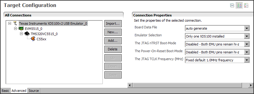
Connected all JTAG cabling, created the CCS target configuration as

Texas Instruments XDS100v2 USB Emulator_0 -> TMS320C5515_0 -> C55xx

and placed the c5515.gel initialization script file that is provided with the collaterals.

When I try to connect to target though I get

"Error connecting to the target:
Error 0x80000240/-183
Fatal Error during: Initialization, OCS,"


Is there a procedure for attaching the XDS100 v2 to the FDK or only the XDS510 is supported?


thanks

Christos


  • Hi Christos,

    Have you tried changing the Clock frequency to "Adaptive Clocking Speed" for XDS100V2?

    Regards,

    Sid

  • Hi Sid,


    Yes I placed a user psecified limit of 1MHz with adaptive freq., I also tried combinations of EM0/EM1 pins (high / low / high-z) but the same error gets out.

    I would like to know if someone is succesful with the XDS100 v2 on fdk.


    Thanks

    Christos


  • Hello Christos,

    I have the luxury of having 4 different XDS100 emulators at my desk. I was able to connect the FDK to each of them (after a little fuss). When creating the target configuration, I selected "EVM5515" as the target and left everything else as default. See screen shot below.

    Many times I saw the error "240/-1063: Bad Silicon Target", but after jiggling the connection, resetting the emulator, and trying again, I was able to connect with each emulator.

    Only twice did I see your error "240/-183: Fatal Error during: Initialization, OCS"
    1) I had setup the target configuration as XDS100v2 when actually connecting through an XDS100v1
    2) I purposely reversed the pin polarity on an XDS100v2. There was no key to prevent me.

    The JTAG adapter that plugs into the FDK seems a little loose. Maybe that was the cause of my "240/-1063: Bad Silicon Target" errors, but in short time I was able to connect reliably.

    Also, when I setup the target configuration for the wrong XDS100 version, I sometimes was not able to connect. Try connecting with both.

    Does your XDS100v2 emulator connect to any other JTAG device? Double check your schematics.

    For your reference, I have copied my tests and a screen shot of my successful target configuration below.

    Hope this helps,
    Mark

    --------------------------------------------------------------------------------------------------   

    "USB100-HS" Board

    Connection = XDS100v1:
        240/-1063: Bad Silicon Target
        Connected!
       
    Connection = XDS100v2:
        240/-183: Fatal Error during: Initialization, OCS
        240/-1041: Device driver: Problem with the Emulation Controller
       
    --------------------------------------------------------------------------------------------------   

    "XDS100v2" Board

    Connection = XDS100v1:
        240/-1063: Bad Silicon Target
       
    Connection = XDS100v2:
        Connected!
       
    --------------------------------------------------------------------------------------------------   

    "Spectrum Digital XDS100" Board

    Connection = XDS100v1:
        Connected!
       
    Connection = XDS100v2:
        Connected!
       
    --------------------------------------------------------------------------------------------------   

    "Olimex XDS100" Emulator

    Connection = XDS100v1:
        240/-1063: Bad Silicon Target
        Connected!
       
    Connection = XDS100v2:
        240/-1063: Bad Silicon Target
        Connected!
       
    --------------------------------------------------------------------------------------------------   

    "Spectrum Digital XDS510" Emulator

    Connection = XDS510:
        Connected!


    --------------------------------------------------------------------------------------------------   

  • Hi Mark,


    Thanks for the detailed answer.

    The JTAG connector on fdk is indeed 'flakey' so extra caution is given there.

    Yet the XDS100v2 that I have still cannot work.

    Its working ok though with a BeagleBoard having the OMAP3530 which is a good test for its working condition I think.


    When I tested on fdk with the settings you provided I got

    Configured as XDS100v1

    "C55xx: Error connecting to the target: Error 0x80000240/-1063 Fatal Error during: Initialization, OCS,  Bad Target Silicon Revision Number Please check your multi-processor configuration. The number of devices in the JTAG scan path must be correct for the silicon revision to be read. Or, you may have selected the wrong DSP device driver. "

    that error comes every time even when I retry/power cycle multiple times.

    Configured as XDS100v2

    "C55xx: Error connecting to the target: Error 0x80000240/-183 Fatal Error during: Initialization, OCS, "

    and then when I clicked retry

    "C55xx: Error connecting to the target: Error 0x80000240/-1041 Fatal Error during: Initialization, OCS,  Device driver: Problem with the Emulation Controller. It is recommended to RESET EMULATOR.  This will disconnect each  target from the emulator.  The targets should then be power cycled or hard reset followed by an emureset and reconnect to each target. "


    These results come always nomater what.


    I do not know why this happens, yet the XDS100 v2 that I use comes from Embest/Timll and it is a 100% reference design, I even downloaded the SD CPLD program ( http://support.spectrumdigital.com/ccs40/xds100v2/ ) myself to be sure and it reported succesful after testing and loading.

    The XDS100 I use is this

    http://www.embedinfo.com/English/product/xds100.asp


    Anyway, I do not want to move at the moment with any emulator than a XDS100 (eg XDS510) since that would altered the CCS license and pricing.

    So, I'll order one XDS100 from SD and I guess it will be ok. As I see from your tests it was the one with the least of problems.


    Thanks again,

    Christos


  • Mark,


    I did some investigation since the XDS100 that I have although it is not working with the FDK it does work with the OMAP3530.


    I've focused and checked the FDK Mini Converter Board for the JTAG (1.27mm to 2.54mm). I checked its electrical continuity beteween the 2.54mm connector and the equivalent pins of the 1.27 connector.

    I've found that pins 4, 6, 10, 12 do not conduct between the two connectors although the board gerber shows that they should connect. The pin 6 is the NC, but the 4, 8, 10,12 are the ground pins, from them thus only the 8 does conduct between connectors.

    Could this be the problem, is pin 8 enough for gnd?


    Christos


  • Christos,

    I noticed that the soldering on my FDK Mini JTAG Converter is also a little "cold"... Maybe you could try melting those pins a little more and testing the connection before you buy another emulator...

    I tried resoldering my JTAG converter with hopes that the 240/-1063: Bad Silicon Target error would stop appearing, but it remains. I'm still able to connect after a second try, however.

    Give it a try and let us know.

    Thanks,
    Mark

  • Mark,

    Please, do me a favor, see also in your own


    FDK Mini JTAG Converter,


    if all pins have one-to-one electrical connection from one connector (2.54mm) to another (1.27mm) on the equivalent pins.

    It seems to me that there is no cold solder, but the actual pcb traces for those pins under the 1.27mm connector going between the connector pads, I think they might have a defect, their width looks like half a mil or non existent at all.


    Tomorrow I'll do a bit of rework on the little converter board.


    Thanks,

    Christos

  • Christos,

    I've got very good connectivity between all pins (except the key).

    The traces do get pretty small to sneak past vias of the the 1.27mm header.

    Let us know if you trace down the problem. Hopefully we can get an XDS100 onboard emulator in the next FDK revision.

    Regards,
    Mark

  • Mark,


    Rework on the conversion pcb has done and here are the results


    XDS100v2->EVM5515 (default .gel)

    C55xx: GEL Output: Reset Peripherals is complete.
    C55xx: GEL Output: Configuring PLL (100.00 MHz).
    C55xx: GEL Output: PLL Init Done.
    C55xx: GEL Output: SDRAM Initilization Complete.
    C55xx: GEL Output: Target Connection Complete.


    XDS100v2->TMS320C5515->c5515.gel (from collaterals) this config gives the EVM5505 gel scripts

    C55xx: GEL Output: Configure PLL (100.00 MHz).
    C55xx: GEL Output: Wait until TESTLOCKMON is high...
    C55xx: GEL Output: After checking TESTLOCKMON bit...
    C55xx: GEL Output: PLL Init Done (100.00 MHz).
    C55xx: GEL Output: Target Connection Complete.


    The output from all gel scripts
    C55xx: GEL Output: SDRAM Initilization Complete.

    C55xx: GEL Output: CPU Reset Complete.

    C55xx: GEL Output: C5505EVM Initialization Complete.

    C55xx: GEL Output: Configure PLL (12.288 MHz).
    C55xx: GEL Output: Wait until TESTLOCKMON is high...
    C55xx: GEL Output: After checking TESTLOCKMON bit...
    C55xx: GEL Output: PLL Init Done (12.288 MHz).

    C55xx: GEL Output: Configure PLL (40.04 MHz).
    C55xx: GEL Output: Wait until TESTLOCKMON is high...
    C55xx: GEL Output: After checking TESTLOCKMON bit...
    C55xx: GEL Output: PLL Init Done (40.04 MHz).

    C55xx: GEL Output: Configure PLL (60.00 MHz).
    C55xx: GEL Output: Wait until TESTLOCKMON is high...
    C55xx: GEL Output: After checking TESTLOCKMON bit...
    C55xx: GEL Output: PLL Init Done (60.00 MHz).

    C55xx: GEL Output: Configure PLL (75.00 MHz).
    C55xx: GEL Output: Wait until TESTLOCKMON is high...
    C55xx: GEL Output: After checking TESTLOCKMON bit...
    C55xx: GEL Output: PLL Init Done (75.00 MHz).

    C55xx: GEL Output: Configure PLL (100.00 MHz).
    C55xx: GEL Output: Wait until TESTLOCKMON is high...
    C55xx: GEL Output: After checking TESTLOCKMON bit...
    C55xx: GEL Output: PLL Init Done (100.00 MHz).

    C55xx: GEL Output: Configure PLL (120.00 MHz).
    C55xx: GEL Output: Wait until TESTLOCKMON is high...
    C55xx: GEL Output: After checking TESTLOCKMON bit...
    C55xx: GEL Output: PLL Init Done (120.00 MHz).

    C55xx: GEL Output: Reset Peripherals is complete.

    Now after the remedy on the FDK Mini-Converter Board, it worked on first try, no complain whatsoever.


    The rework was to solder small wires between the two connectors for pins 2,4,8,10,12,14.

    These pins have defect pcb traces (at least on mine) underneath the 1.27mm connector and there is no conductivity or conductivity with resistance (pin 8 ~0.5 Ohm).


    Christos


  • The remedy on FDK Mini-Converter Board


    Christos


  • Christos,

    Nice soldering job!

    I'll bring up this issue with the PCB manufacturer.

    Thanks,
    Mark