This thread has been locked.

If you have a related question, please click the "Ask a related question" button in the top right corner. The newly created question will be automatically linked to this question.

OMAP-L138: problem of using Flash Loading Utility for booting OMAP

Part Number: OMAP-L138
Other Parts Discussed in Thread: OMAPL138,

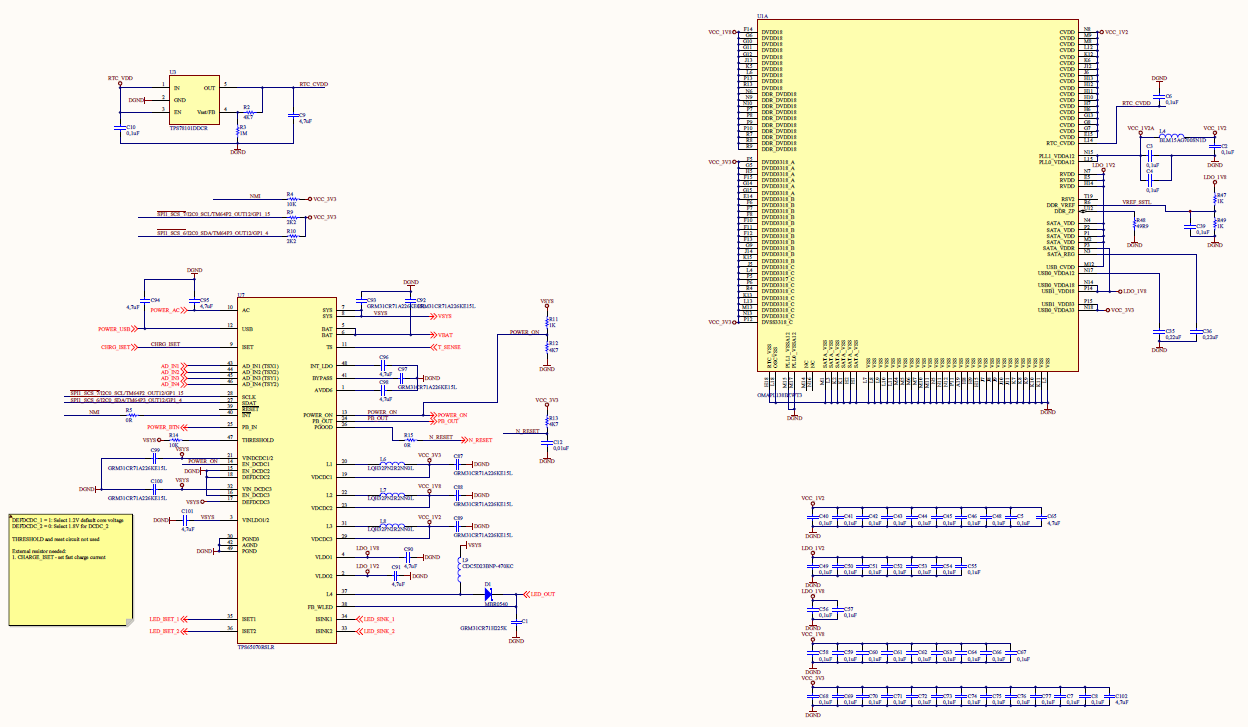
 I'm using a OMAPL138 processor board. I have 2 different board. The electrical circuit for the first board is on the pictures

The electrical circuit for the secondt board is on the pictures

I booting both boards the processor OMAP-L138_FlashAndBootUtils_2_40 utility by UART2 interface. I booting *.ais file to NAND flash. I download OMAP-L138_FlashAndBootUtils_2_40 utility from https://sourceforge.net/projects/dvflashutils/files/OMAP-L138/v2.40/.

Furser, I set the boot pins to UART2 boot mode. And I enter command in the console for erasing NAND flash: sfh_OMAP-L138.exe -erase -targetType OMAP-L138 -flashType NAND -p COM4 -v.

I see on the console log for first board

-----------------------------------------------------
   TI Serial Flasher Host Program for OMAP-L138
   (C) 2017, Texas Instruments, Inc.
   Ver. 1.67
-----------------------------------------------------
 
      [TYPE] Global erase
    [TARGET] OMAPL138
    [DEVICE] NAND
    [NAND Block] 1
Attempting to connect to device /dev/ttyUSB0...
Press any key to end this program at any time.
(AIS Parse): Read magic word 0x41504954.
(AIS Parse): Waiting for BOOTME... (power on or reset target now)
(AIS Parse): BOOTME received!
(AIS Parse): Performing Start-Word Sync...
(AIS Parse): Performing Ping Opcode Sync...
(AIS Parse): Processing command 0: 0x58535901.
(AIS Parse): Performing Opcode Sync...
(AIS Parse): Loading section...
(AIS Parse): Loaded 14100-Byte section to address 0x80000000.
(AIS Parse): Processing command 1: 0x58535901.
(AIS Parse): Performing Opcode Sync...
(AIS Parse): Loading section...
(AIS Parse): Loaded 1352-Byte section to address 0x80003714.
(AIS Parse): Processing command 2: 0x58535906.
(AIS Parse): Performing Opcode Sync...
(AIS Parse): Performing jump and close...
(AIS Parse): AIS complete. Jump to address 0x80000000.
(AIS Parse): Waiting for DONE...
(AIS Parse): Boot completed successfully.
Waiting for SFT on the OMAP-L138...
    Target: BOOTUBL
    Target:    DONE
    Target:    SIZE
    Target: 00000001
Erasing flash
   0% [ ------------------------------------------------------------ ]
 100%   ████████████████████████████████████████████████████████████ 
 100%   ████████████████████████████████████████████████████████████ 
                            Erase complete                           
    Target:    DONE
    Target:    DONE
And I see for second board
-----------------------------------------------------
   TI Serial Flasher Host Program for OMAP-L138
   (C) 2017, Texas Instruments, Inc.
   Ver. 1.67
-----------------------------------------------------
 
      [TYPE] Global erase
    [TARGET] OMAPL138
    [DEVICE] NAND
    [NAND Block] 1
Attempting to connect to device /dev/ttyUSB0...
Press any key to end this program at any time.
(AIS Parse): Read magic word 0x41504954.
(AIS Parse): Waiting for BOOTME... (power on or reset target now)
(AIS Parse): BOOTME received!
(AIS Parse): Performing Start-Word Sync...
(AIS Parse): Performing Ping Opcode Sync...
(AIS Parse): Processing command 0: 0x58535901.
(AIS Parse): Performing Opcode Sync...
(AIS Parse): Loading section...
(AIS Parse): Loaded 14100-Byte section to address 0x80000000.
(AIS Parse): Processing command 1: 0x58535901.
(AIS Parse): Performing Opcode Sync...
(AIS Parse): Loading section...
(AIS Parse): Loaded 1352-Byte section to address 0x80003714.
(AIS Parse): Processing command 2: 0x58535906.
(AIS Parse): Performing Opcode Sync...
(AIS Parse): Performing jump and close...
(AIS Parse): AIS complete. Jump to address 0x80000000.
(AIS Parse): Waiting for DONE...
(AIS Parse): Boot completed successfully.
Waiting for SFT on the OMAP-L138...
    Target: BOOTUBL
    Target:    DONE
The programm does not end.
Furser, I looked with an oscilloscope NAND port pins on second board and I  don't looked timing diagramm for NAND flash. All processor pins for NAND is set 3.3V. But, I'm look correct timing diagramm on oscilloscope for first board.
What is the problem?
  • Hi Alexey,

    Our team will need some time to analyze the issue. Please allow us a few days and we will get back to you.

    BR
    Tsvetolin Shulev
  • Hello

    Did you understand my question?

  • I have not received an answer to my question, many days passed. Wait do I answer?

  • Hello. Sorry, I did not see this question until today.

    I understand that the first board programs the NAND flash with the Serial Flasher tool, but the second board stops at the stage where the NAND is erased.

    On the second board, have you confirmed voltages are up, clocks toggling, and reset is going to high?

    You should also have checked your schematics against this Schematic Review Checklist:
    processors.wiki.ti.com/.../_AM1x_Schematic_Review_Checklist
    Compare also to the EVM for the OMAP L-138: www.ti.com/.../tmdslcdk138

    I only briefly checked the schematics, but I noticed on both boards that the JTAG implementation is not correct. TRST should be pulled low and EMU1 and EMU0 should be pulled high. I'm not sure how the first board worked with these issues. Are you able to connect to the processor with JTAG and run programs? Can you run any NAND test through JTAG?

    On the second board, I'd say the connections to the NAND flash look okay. What is the NAND device used on the first board that works?

    Anyway, it looks as if the serial flasher is communicating with the OMAP-L138 device, but it is hanging at the stage where it communicates with the NAND flash. Did you say you probed the signals going to the NAND but saw no activity? Is there any communication at all? Can you share the waveforms of CSn, CLE, ALE, WEn, and REn?

    Let me also check with a colleague more familiar with the Serial Flasher to see if he recognizes the error.

    Regards,
    Mark
  • Alexey,

    The serial flashing utility also has dependency on DDR as the utility loads a flashing binary into DDR and loads the boot image into device memory and then flashes the NAND, have you also checked out that the DDR connections to EMIF are good?

    While the serial flashing utility is convenient way to flash the device, it is harder to debug so as Mark mentioned, I would run some basic diagnostics over JTAG before attempting to debug the issue with SFH. There is a NANDWriter CCS project that we provide with the Serial and flashing tools which you can import but you need compiler CGT 7.4.x to be able to build it, which you caan get from here:
    software-dl.ti.com/.../download.htm

    Regards,
    Rahul
  • On work board used NAND flash K9F4G08U0D-SIB0000.The Flash Loading Utility is correct work with that NAND. I toggled GPIO of power banks A and C on second board, this GPIO's is work as GPIO

  • Hi Alexey,

    Have you verified the DDR2 is working on the second board? As Rahul pointed out, there is a dependency on DDR for the Serial Flashing Utility to work right.

    Can you test the DDR2 operation by using diagnostics loaded with JTAG from CCS?

    If the layout is not done carefully, DDR might not work properly. I looked at the schematics, and they appear to be okay.

    Regards,
    Mark

  • Hi

    I tested the DDR2 operation by using diagnostics loaded with JTAG from CCS on the second board. DDR is work OK.

  • Alexey,

    Thanks for following up. Can we close this thread now? Or is there still an issue?

    Regards,
    Mark