This thread has been locked.

If you have a related question, please click the "Ask a related question" button in the top right corner. The newly created question will be automatically linked to this question.

RTOS: K2GEVM PCM1684 configurtation

Other Parts Discussed in Thread: PCM1864

Tool/software: TI-RTOS

Before we test the K2GEVM board  ,we find the configuartion information in realtime_demo_bios is conflictd with《PCM186x 103 dB 2ch and 4ch Audio ADCs With Universal Front End》reference information(page-31).The Master  configurations of  PCM1864 in the realtime_demon_bios  is as follow:

ret = cmb_pcm186x_write_reg(addr, 0x00, 0x00);

ret |= cmb_pcm186x_write_reg(addr, 0x20, 0x3E);  // {0x21, 0x0B}, // PLL to DSP1 Divide value = 1/12
ret |= cmb_pcm186x_write_reg(addr, 0x21, 0x0B);  // {0x22, 0x17}, // PLL to DSP2 Divide value = 1/24
ret |= cmb_pcm186x_write_reg(addr, 0x22, 0x17);   // {0x23, 0x2F}, // PLL to ADC Divide value = 1/48
ret |= cmb_pcm186x_write_reg(addr, 0x23, 0x2F);


ret |= cmb_pcm186x_write_reg(addr, 0x20, 0x30);  // {0x20, 0x30}
ret |= cmb_pcm186x_write_reg(addr, 0x21, 0x02); // {0x21, 0x02}, // XTAL to DSP1 Divide value = 1/3
ret |= cmb_pcm186x_write_reg(addr, 0x22, 0x05); // {0x22, 0x05}, // XTAL to DSP2 Divide value = 1/6
ret |= cmb_pcm186x_write_reg(addr, 0x23, 0x0B);// {0x23, 0x0B}, // XTAL to ADC Divide value = 1/12
ret |= cmb_pcm186x_write_reg(addr, 0x25, 0x17); // {0x25, 0x17}, // PLL to SCK Divide value = 1/24
ret |= cmb_pcm186x_write_reg(addr, 0x26, 0x03);// {0x26, 0x03}, /** SCK to BCK divider to 4 **/

ret |= cmb_pcm186x_write_reg(addr, 0x29, 0x03);// {0x29, 0x03} P Divide value = 1/4

ret |= cmb_pcm186x_write_reg(addr, 0x2a, 0x00);// {0x2a, 0x00} R Divide value = 1

ret |= cmb_pcm186x_write_reg(addr, 0x2b, 0x10);// {0x2b, 0x10} J Divide value = 16

ret |= cmb_pcm186x_write_reg(addr, 0x28, 0x01);// {0x28, 0x01} PLL_REF_SEL=SCK; PLL_EN=Enabled

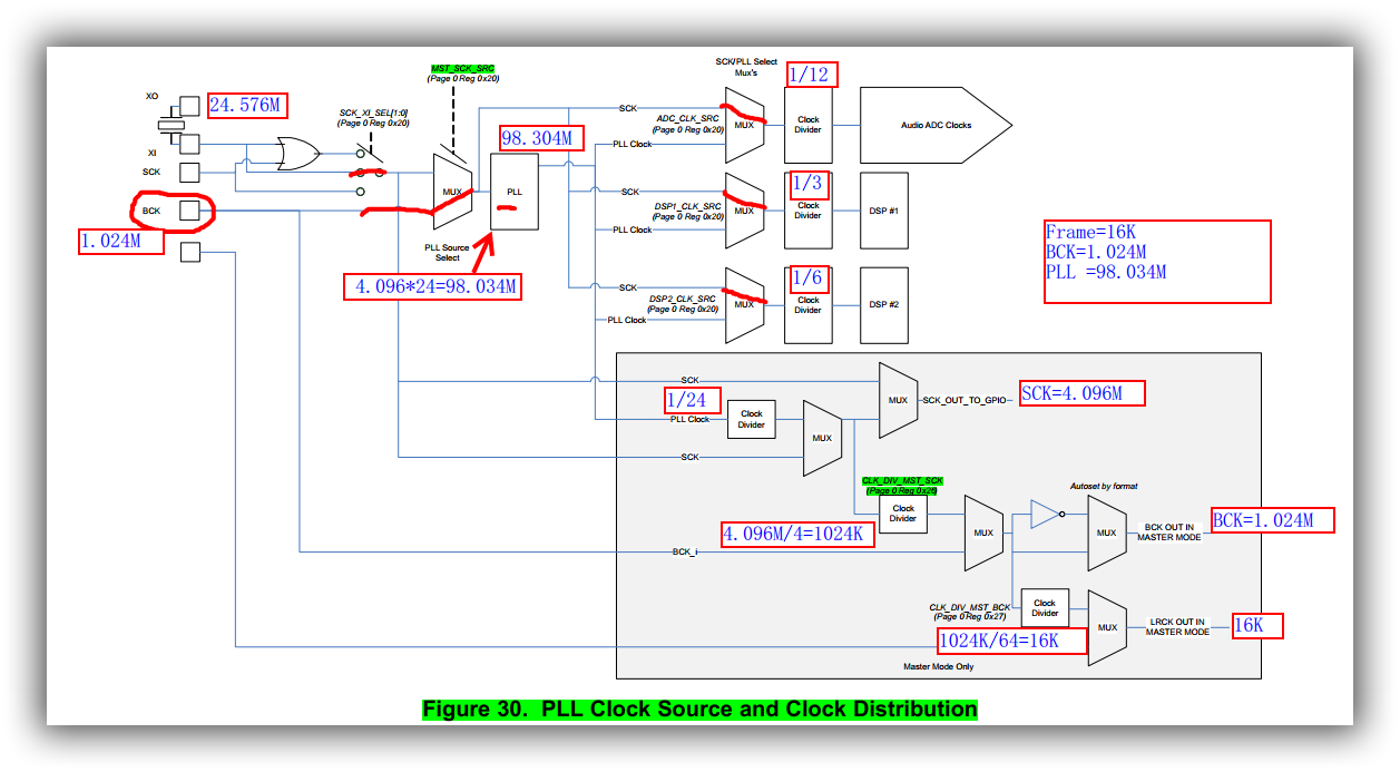
we cann't   figure out  Master clock  number ,  Bit clock number and Frame  clock nubmer . Is  the bit clock offered  by the pin of K2G SOC_MCASP1ACLKR( JP1-33 ) ?

We are  confused on this problem. We are waiting  for your help.

 Thank you very much !


   Wujun 

  • The team is notified. They will post their feedback directly here.

    BR
    Tsvetolin Shulev
  • Wujun,

    Yes, that's correct. K2G SOC_MCASP1ACLKR is the Bit clock.

    Lali

  • Lali

    I have several questions .

    question 1. The bit from pin K2G SOC_MCASP1ACLKR is 1.024MHz(  16KHz*32bit*2 =1024K), is it right ?

    question 2.  from the  ret |= cmb_pcm186x_write_reg(addr, 0x20, 0x30), we know that  PLL source  is BCK , BCK is  1.024 MHz ,from   configuration list

                       ret |= cmb_pcm186x_write_reg(addr, 0x25, 0x17);// {0x25, 0x17}, // PLL to SCK Divide value = 1/24

                       ret |= cmb_pcm186x_write_reg(addr, 0x26, 0x03);// {0x26, 0x03}, /** SCK to BCK divider to 4 **/

                      ret |= cmb_pcm186x_write_reg(addr, 0x29, 0x03);// {0x29, 0x03} P Divide value = 1/4

                      ret |= cmb_pcm186x_write_reg(addr, 0x2a, 0x00);// {0x2a, 0x00} R Divide value = 1

                      ret |= cmb_pcm186x_write_reg(addr, 0x2b, 0x10);// {0x2b, 0x10} J Divide value = 16

                     we can calculate  the SCK is 4.096MHz ( 1.024*R*J.D/P = 1.024*1*16.0/4 =4.096) . PLL clock output is 98.034M ( 4.096*24=98.034);   is   it  right ?

    question3 ,SCK_OUT_TO_GPIO is 4.096 MHz ( 98.034/24) , Bit Clock is 1.024MHz (4.096M/4 =1.024 ),  LRCK OUT clock  is16K (1.024M/64 =16K) , is it right ?

     if  there are mistakes in the calculations , please point out and show us how to calculate . Thank you for your help .  

  • Wujun,
    Yes, your answers to the 3 questions are correct!

    Lali
  • Lali

    Thank you very much !

     Wujun