This thread has been locked.

If you have a related question, please click the "Ask a related question" button in the top right corner. The newly created question will be automatically linked to this question.

TMS320C6678: L2 cache/ram memory access latency

Part Number: TMS320C6678


Dear Champs,

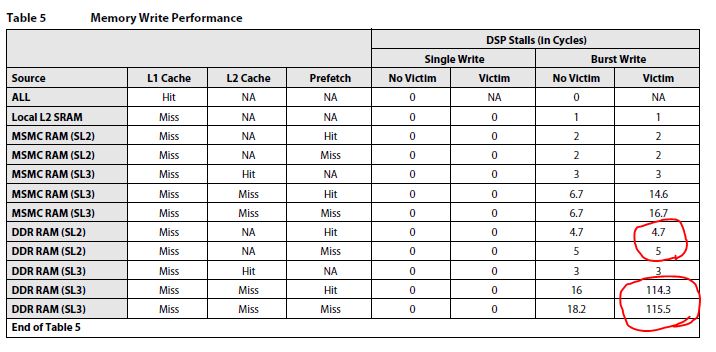
My customer is looking for the data of L2 memory latency.

Could you please let me know the L2 cache/ram, MSMC memory and external DDR3 memory latency of C6678?

And also, when core0 access to L2 cache/ram of core1, what is the memory latency in this case?

Thanks and Best Regards,

SI.

  • Hi,

    I've notified the RTOS team. They will post their feedback directly here.

    Best Regards,
    Yordan
  • Sung-IL,
    There are multiple aspects, can you clarify if customer is trying to understand the following:
    1. L2 cache miss latency
    2. L2 RAM latecy for both code and data
    3. MSMC RAM latency for both code and data
    4. External DDR latency
    jian
  • Hi Jian,

    I found these data in 'Throughput Performance Guide', but did not find any data when access it of other cores.

    Could you please let me know if the latency when core0 access L2 SRAM of core1 in C6678?

    And, in the table5 Memory Write Performance of 'Throughput Performance Guide for TCI66x KeyStone Devices'(sprabh2a.pdf), Could you please explain why there is big difference between DDR RAM(SL2) and DDR RAM(SL3) for Victim?

    And what is the difference between 'No Victim' and 'Victim' in this case?

    Thanks and Best Regards,

    SI.

  • Sung-IL,

    On the latency to access another core's L2, it will be similar to DDR RAM situation, as Core0 has to first go out to MSMC->TeraNet->Core1_L2, as shown in Figure 1 of the same document. For example, if Core1 L2 is configured as SL3 to Core0, it may be ~100 CPU cycles with burst write when both Core0 caches miss.

    On the burst write difference between DDR-RAM SL2 vs. SL3 - SL3 mode, cache lines with victim in L2 are to be read back and merged, that's why you see a large number of 115.5 cycles. In SL2 mode, the L2 cache is disabled, so the L1D cache miss is passed directly to DDR. In this case, since L1D does not write allocate (it does not allocate a cache line), therefore, there is no read back and merging to L1 cache lines, that's why you see the burst write to DDRRAM-SL2 show no cycle difference.

    let me know if this clear, or you need more precise cycle estimates for L2 access from another core. It is only practical in very limited software design to use neighbor's L2.

    Jian
  • Sung-IL,
    i will close this ticket to comply with our internal tracking. please re-open if you have more questions.
    Jian