This thread has been locked.

If you have a related question, please click the "Ask a related question" button in the top right corner. The newly created question will be automatically linked to this question.

AM5726: PET questions

Part Number: AM5726
Other Parts Discussed in Thread: AM5728

Hi,

I have question about PET setting for AM 572x.


Q1: For MPU profile, idle, dhrystone, max can be selected, what is the difference between these configurations?
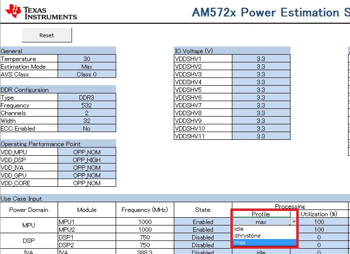

Q2: For DSP profile, idle, typ, max can be selected, what is the difference between these configurations?


Best regards,
H.U

  • The PET experts have been notified. They will respond here.
  • "Max" is a profile for worst case power that is not realistically achievable in any use case. It is characterized on a chip tester that enables everything on the chip at once. You can use that for power supply sizing and PCB voltage drop simulations. "Typ" or "Dhrystone" is when the IP is active performing some operation. MPU is running dhrystone, DSP is running an openCL application, IVA is decoding HD video, GPU is running an openGL application, DMA, PCIE, SD card, or USB drive is transferring data, etc. Then "Idle" is just enabled.
  • Thank you for your reply.
    Please forgive me any additinal questions.

    Q3: Should we do thermal design also using the "MAX" profile?

    Q4: We measured the current consumption using AM572xEVM.
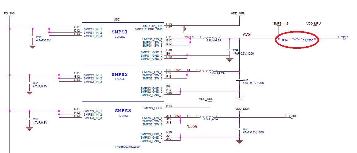
    Our test code drives two A15 cores at full performance, probing at R34 in the figure below, the observed current consumption was 2450.0 mA.
    It was close to the worst case (2608 mA) with PET. Please see the attached spreadsheet. SPRACA0_AM572x_Power_Spreadsheet_v1p4p1.zip
    The measured current value greatly exceeds the calculated value in the drystone profile, is this supposed value?


    Best regards,
    H.U

  • Q3. The tool is for estimation purposes only. Nothing is better than real world testing on a prototype. 

    Q4. Dhrystone stresses the integer units of a CPU, it's possible your test code stresses the float point units and relies on memory bandwidth as well. Dhrystone is an old program we keep due to legacy and familiarity. 

  • Hi Ahmad_Rashed,

    Q4 : Our test code is rarely using floating point unit,
    Even in a general use case, actual power consumption may exceed the calculated value in dhrystone profile of PET, is that supposed to be assumed?
    We are confused as to which profile settings should be used to design for the power supply.

    Best regards,
    H.U

  • Hi Ahmad_Rashed,

    Q5:We measured the power consumption of the DSP core with VDD_DSP power rail at R35. Driving the two C66x cores at full performance with max frequency (750Mhz), it was 550 mA.
    However, PET shows that when using Utilization to 100% with typ profile, it becomes 1154 mA.
    Why is the measured result and the estimation result greatly different?

    Best regards,
    H.U
  • I see in the spreadsheet provided you have the MPU @ OPP_NOM and the DSP @ OPP_HIGH. What are you using to control the state? Can you give me the voltage measurement in addition to the current? Do you have a tool for reading the die temperature as well? 

  • Hi Ahmad_Rashed,

    We are tested it using that the MPU is OPP_NOM state and the DSP is OPP_HIGH state. I can share our test code, Could you confirm it?
    For the voltage measurement, the VDD_MPU was 1.100 V, the VDD_DSP was 1.091 V.
    When running the test code, the chip was quite hot, did you need temperature measurement?

    Best regards,
    H.U

  • It is possible the core temperature is higher than 65C... the AM57xx power is sensitive to high temperatures. Use the command below to get internal die temperature. 

    omapconf show temp

    I also don't think the MPU is running at NOM because 1.100V sounds too high. To confirm, can you also read the value of this register: 0x4a003b20

    devmem2 0x4A003B20 w

    The value in the first 3 bytes tells you what the MPU voltage should be at NOM. What you measure on the board will be ~150mV higher due.

    To make sure OPP_OD and OPP_HIGH are disabled, you need to remove them from the dra7.dtsi.

  • Hi Ahmad_Rashed,

    Our test code is based on Processor SDK RTOS. Therefore, we can not try the commands supported by Linux.Is there any other way to check the die temperature?

    Since the previously presented voltage value was wrong, I will correct it below.

    VDD_MPU = 1.076 mV
    VDD_DSP = 1.086 mV

    We will check the value of 0x4A003B20 and get back to you.

    We expect you to experiment in your EVM environment with our test program.
    Or could you tell me the actual value of the power consumption when driving A15 * 2 and C66x * 2 cores of AM5728 with 100% utilization?


    Best regards,
    H.U

  • There is a GEL script that comes with CCS and it is capable of reading the die temperatures. You can also make your own RTOS application by using the code in the GEL script as reference. The script location is "ccsv7\ccs_base\emulation\boards\am572x\gel\AM572x_prcm_config.gel"

  • Hi Ahmad_Rashed,

    I will present the temperature information followed by GEL, this temperature value was acquired after executing the test program for 30 minutes.
    In addition, 0x4A003B20 information is also shown below.

    MPU Temperature: 70 degC
    GPU Temperature: 67 degC
    CORE Temperature: 67 degC
    IVA Temperature: 68 degC

    CTRL_CORE_STD_FUSE_OPP_VMIN_MPU_2(0x4A003B20) = 0x03D00401
    CTRL_CORE_STD_FUSE_OPP_VMIN_MPU_3(0x4A003B24) = 0x03B00445
    CTRL_CORE_STD_FUSE_OPP_VMIN_MPU_4(0x4A003B28) = 0x039004A4


    I recalculated the PET with the temperature setting at 70 , this result seems to be very different from the measured value. see attached file.SPRACA0_AM572x_Power_Spreadsheet_v1p4p1_at_ourtestprogram.zip
    Please tell me the reason why this difference occur.
    My customer must immediately clear this problem for their board thermal design. So we need your help.


    Best regards,
    H.U

  • In the PET, you have the DSP running at OPP high (750MHz @ 1.22V) but earlier the voltage you measured was under 1.10V. That is likely the reason for difference in power on the DSP.

    Are you familiar with the RTOS Power Management driver? You should use that to make sure your voltages and frequencies are set correctly since that is a critical part to keeping within your power and heat budget. See <pdk-install-dir>\ti\drv\pm\ for finding examples and documentation. 

  • Hi Ahmad_Rashed,

    Are you say that PET is calculated assuming that 1.22 V is supplied to VDD_DSP when the DSP runing at OPP high?
    If the actual VDD_DSP voltage is low even when OPP is High, does it means that the difference will be nearly two times lower than the calculation result of PET?

    Our test program is started from MMCSD boot. So, the ower management and clock setting are done by SBL.


    Voltage setting changed from line 506 of "sbl_avs_config.c".
    Please see attached file.

    /**
     *  \file   sbl_avs_config.c
     *
     *  \brief  This file contains functions and data related to AVS and ABB
     *          configuration for the voltage rails.
     *
     */
    
    /*
     * Copyright (C) 2015-2017 Texas Instruments Incorporated - http://www.ti.com/
     *
     * Redistribution and use in source and binary forms, with or without
     * modification, are permitted provided that the following conditions
     * are met:
     *
     * Redistributions of source code must retain the above copyright
     * notice, this list of conditions and the following disclaimer.
     *
     * Redistributions in binary form must reproduce the above copyright
     * notice, this list of conditions and the following disclaimer in the
     * documentation and/or other materials provided with the
     * distribution.
     *
     * Neither the name of Texas Instruments Incorporated nor the names of
     * its contributors may be used to endorse or promote products derived
     * from this software without specific prior written permission.
     *
     * THIS SOFTWARE IS PROVIDED BY THE COPYRIGHT HOLDERS AND CONTRIBUTORS
     * "AS IS" AND ANY EXPRESS OR IMPLIED WARRANTIES, INCLUDING, BUT NOT
     * LIMITED TO, THE IMPLIED WARRANTIES OF MERCHANTABILITY AND FITNESS FOR
     * A PARTICULAR PURPOSE ARE DISCLAIMED. IN NO EVENT SHALL THE COPYRIGHT
     * OWNER OR CONTRIBUTORS BE LIABLE FOR ANY DIRECT, INDIRECT, INCIDENTAL,
     * SPECIAL, EXEMPLARY, OR CONSEQUENTIAL DAMAGES (INCLUDING, BUT NOT
     * LIMITED TO, PROCUREMENT OF SUBSTITUTE GOODS OR SERVICES; LOSS OF USE,
     * DATA, OR PROFITS; OR BUSINESS INTERRUPTION) HOWEVER CAUSED AND ON ANY
     * THEORY OF LIABILITY, WHETHER IN CONTRACT, STRICT LIABILITY, OR TORT
     * (INCLUDING NEGLIGENCE OR OTHERWISE) ARISING IN ANY WAY OUT OF THE USE
     * OF THIS SOFTWARE, EVEN IF ADVISED OF THE POSSIBILITY OF SUCH DAMAGE.
     *
     */
    
    #include "sbl_avs_config.h"
    #include "sbl_prcm.h"
    
    #include <ti/csl/cslr_device.h>
    #include <ti/csl/hw_types.h>
    #include <ti/board/board.h>
    #include <ti/drv/pm/pmhal.h>
    #if defined(idkAM572x)
    #include <ti/board/src/idkAM572x/device/pmic_device.h>
    #elif defined(idkAM571x)
    #include <ti/board/src/idkAM571x/device/pmic_device.h>
    #elif defined(evmAM572x)
    #include <ti/board/src/evmAM572x/device/pmic_device.h>
    #elif defined(idkAM574x)
    #include <ti/board/src/idkAM574x/device/pmic_device.h>
    #endif
    
    /**********************************************************************
    ************************** Internal functions ************************
    **********************************************************************/
    
    /**
     * \brief    SBL_Read_Efuse_Reg function to read the voltage value from efuse
     *
     * \param    railVoltage pointer to the rail voltage.
     *
     * \retval   regVal  Value from the Efuse registers.
     *
     **/
    static uint32_t SBL_Read_Efuse_Reg(const voltage_rail_t *railVoltage);
    
    /**
     * \brief     SBL_GetOppConfig function to get the 
     *
     * \param     oppVal   value representing the OPP mode.
     * \param     boardId  Board ID value
     *
     * \retval    voltCoreData   pointer to the AVS data for the particular OPP.
     *
     **/
    static const vcores_data_t* SBL_GetOppConfig(uint32_t oppVal, uint32_t boardId);
    
    /**
     * \brief     Initialize the I2C controller by configuring the pinmux and
     *            module clocks.
     *
     * \param     oppVal   value representing the OPP mode.
     *
     **/
    static void SBL_I2CInit();
    
    /**
     * \brief     Function to resolve the Board Name string to BoardId.
     * 
     * \param     pBoardName  Pointer to the Board Name String.
     *
     **/
    static uint32_t SBL_GetBoardid(char *pBoardName);
    
     /**********************************************************************
     ************************** Macros ************************************
     **********************************************************************/
    
    /* TPS659039 */
    #define TPS659039_I2C_SLAVE_ADDR            0x58
    #define TPS659039_REG_ADDR_SMPS12           0x23
    #define TPS659039_REG_ADDR_SMPS45           0x2B
    #define TPS659039_REG_ADDR_SMPS6            0x2F
    #define TPS659039_REG_ADDR_SMPS7            0x33
    #define TPS659039_REG_ADDR_SMPS8            0x37
    
    #define TPS659039_PMIC_DEV_CTRL             0xA0
    
    /* TPS659039 Voltage settings in mv for OPP_NOMINAL */
    #define VDD_MPU_AM57XX      1100
    #define VDD_DSP_AM57XX      1060
    #define VDD_GPU_AM57XX      1060
    #define VDD_CORE_AM57XX     1030
    #define VDD_IVA_AM57XX      1060
    
    /* Efuse register offsets for DRA7xx platform */
    #define AM57XX_EFUSE_BASE                   0x4A002000U
    #define AM57XX_EFUSE_REGBITS                16
    
    /* STD_FUSE_OPP_VMIN_IVA_2 */
    #define STD_FUSE_OPP_VMIN_IVA_NOM           (AM57XX_EFUSE_BASE + 0x05CC)
    /* STD_FUSE_OPP_VMIN_IVA_3 */
    #define STD_FUSE_OPP_VMIN_IVA_OD            (AM57XX_EFUSE_BASE + 0x05D0)
    /* STD_FUSE_OPP_VMIN_IVA_4 */
    #define STD_FUSE_OPP_VMIN_IVA_HIGH          (AM57XX_EFUSE_BASE + 0x05D4)
    /* STD_FUSE_OPP_VMIN_DSPEVE_2 */
    #define STD_FUSE_OPP_VMIN_DSPEVE_NOM        (AM57XX_EFUSE_BASE + 0x05E0)
    /* STD_FUSE_OPP_VMIN_DSPEVE_3 */
    #define STD_FUSE_OPP_VMIN_DSPEVE_OD         (AM57XX_EFUSE_BASE + 0x05E4)
    /* STD_FUSE_OPP_VMIN_DSPEVE_4 */
    #define STD_FUSE_OPP_VMIN_DSPEVE_HIGH       (AM57XX_EFUSE_BASE + 0x05E8)
    /* STD_FUSE_OPP_VMIN_CORE_2 */
    #define STD_FUSE_OPP_VMIN_CORE_NOM          (AM57XX_EFUSE_BASE + 0x05F4)
    /* STD_FUSE_OPP_VMIN_GPU_2 */
    #define STD_FUSE_OPP_VMIN_GPU_NOM           (AM57XX_EFUSE_BASE + 0x1B08)
    /* STD_FUSE_OPP_VMIN_GPU_3 */
    #define STD_FUSE_OPP_VMIN_GPU_OD            (AM57XX_EFUSE_BASE + 0x1B0C)
    /* STD_FUSE_OPP_VMIN_GPU_4 */
    #define STD_FUSE_OPP_VMIN_GPU_HIGH          (AM57XX_EFUSE_BASE + 0x1B10)
    /* STD_FUSE_OPP_VMIN_MPU_2 */
    #define STD_FUSE_OPP_VMIN_MPU_NOM           (AM57XX_EFUSE_BASE + 0x1B20)
    /* STD_FUSE_OPP_VMIN_MPU_3 */
    #define STD_FUSE_OPP_VMIN_MPU_OD            (AM57XX_EFUSE_BASE + 0x1B24)
    /* STD_FUSE_OPP_VMIN_MPU_4 */
    #define STD_FUSE_OPP_VMIN_MPU_HIGH          (AM57XX_EFUSE_BASE + 0x1B28)
    
    #define CTRL_CORE_PAD_I2C1_SDA                      (0x400U)
    #define CTRL_CORE_PAD_I2C1_SCL                      (0x404U)
    
    #define CTRL_CORE_PAD_I2C1_SCL_PIN_PULLUP_EN        (0x00050000U)
    #define CTRL_CORE_PAD_I2C1_SDA_PIN_PULLUP_EN        (0x00050000U)
    
    #define BOARD_NAME_LENGTH                           (8)
    #define OPP_TABLE_SIZE                              (3)
    
    #if defined(idkAM572x) || defined(idkAM574x)
    /* Structure to hold the AVS values of all voltage rails for OPP NOM */
    const vcores_data_t idkAM572x_opp_nom_volts = {
        {
        VDD_MPU_AM57XX,
        TPS659039_REG_ADDR_SMPS12,
        {
            STD_FUSE_OPP_VMIN_MPU_NOM,
            AM57XX_EFUSE_REGBITS
        },
        },
    
        {
        VDD_CORE_AM57XX,
        TPS659039_REG_ADDR_SMPS7,
        {
            STD_FUSE_OPP_VMIN_CORE_NOM,
            AM57XX_EFUSE_REGBITS
        },
        },
    
        {
        VDD_DSP_AM57XX,
        TPS659039_REG_ADDR_SMPS45,
        {
            STD_FUSE_OPP_VMIN_DSPEVE_NOM,
            AM57XX_EFUSE_REGBITS
        },
        },
    
        {
        VDD_GPU_AM57XX,
        TPS659039_REG_ADDR_SMPS6,
        {
            STD_FUSE_OPP_VMIN_GPU_NOM,
            AM57XX_EFUSE_REGBITS
        },
        },
    
        {
        VDD_IVA_AM57XX,
        TPS659039_REG_ADDR_SMPS8,
        {
            STD_FUSE_OPP_VMIN_IVA_NOM,
            AM57XX_EFUSE_REGBITS
        },
        }
    };
    
    /* Structure to hold the AVS values of all voltage rails for OPP OD */
    const vcores_data_t idkAM572x_opp_od_volts = {
        {
        VDD_MPU_AM57XX,
        TPS659039_REG_ADDR_SMPS12,
        {
            STD_FUSE_OPP_VMIN_MPU_OD,
            AM57XX_EFUSE_REGBITS
        },
        },
    
        {
        VDD_CORE_AM57XX,
        /* core does not support opp OD; using opp NOM */
        TPS659039_REG_ADDR_SMPS7,
        {
            STD_FUSE_OPP_VMIN_CORE_NOM,
            AM57XX_EFUSE_REGBITS
        },
        },
    
        {
        VDD_DSP_AM57XX,
        TPS659039_REG_ADDR_SMPS45,
        {
            STD_FUSE_OPP_VMIN_DSPEVE_OD,
            AM57XX_EFUSE_REGBITS
        },
        },
    
        {
        VDD_GPU_AM57XX,
        TPS659039_REG_ADDR_SMPS6,
        {
            STD_FUSE_OPP_VMIN_GPU_OD,
            AM57XX_EFUSE_REGBITS
        },
        },
    
        {
        VDD_IVA_AM57XX,
        TPS659039_REG_ADDR_SMPS8,
        {
            STD_FUSE_OPP_VMIN_IVA_OD,
            AM57XX_EFUSE_REGBITS
        },
        }
    };
    
    /* Structure to hold the AVS values of all voltage rails for OPP HIGH */
    const vcores_data_t idkAM572x_opp_high_volts = {
        {
        VDD_MPU_AM57XX,
        TPS659039_REG_ADDR_SMPS12,
        {
            STD_FUSE_OPP_VMIN_MPU_HIGH,
            AM57XX_EFUSE_REGBITS
        },
        },
    
        {
        VDD_CORE_AM57XX,
        TPS659039_REG_ADDR_SMPS7,
        /* core does not support opp high; using opp NOM */
        {
            STD_FUSE_OPP_VMIN_CORE_NOM,
            AM57XX_EFUSE_REGBITS
        },
        },
    
        {
        VDD_DSP_AM57XX,
        TPS659039_REG_ADDR_SMPS45,
        {
            STD_FUSE_OPP_VMIN_DSPEVE_HIGH,
            AM57XX_EFUSE_REGBITS
        },
        },
    
        {
        VDD_GPU_AM57XX,
        TPS659039_REG_ADDR_SMPS6,
        {
            STD_FUSE_OPP_VMIN_GPU_HIGH,
            AM57XX_EFUSE_REGBITS
        },
        },
    
        {
        VDD_IVA_AM57XX,
        TPS659039_REG_ADDR_SMPS8,
        {
            STD_FUSE_OPP_VMIN_IVA_HIGH,
            AM57XX_EFUSE_REGBITS
        },
        }
    };
    #endif
    
    /* Structure defining the OPP table for AM572xIDK. */
    boardOppData_t gAm572xIdkOppTable[] =
    {
        #if defined(idkAM572x) || defined(idkAM574x)
        {OPP_MODE_NOM, &idkAM572x_opp_nom_volts},
        {OPP_MODE_OD, &idkAM572x_opp_od_volts},
        {OPP_MODE_HIGH, &idkAM572x_opp_high_volts}
        #endif
    };
    
    #if defined(idkAM571x)
    /* Structure to hold the AVS values of all voltage rails for OPP NOM */
    const vcores_data_t idkAM571x_opp_nom_volts = {
        {
        VDD_MPU_AM57XX,
        TPS659039_REG_ADDR_SMPS12,
        {
            STD_FUSE_OPP_VMIN_MPU_NOM,
            AM57XX_EFUSE_REGBITS
        },
        },
    
        {
        VDD_CORE_AM57XX,
        TPS659039_REG_ADDR_SMPS7,
        {
            STD_FUSE_OPP_VMIN_CORE_NOM,
            AM57XX_EFUSE_REGBITS
        },
        },
    
        /* DSP rail not connected for idkAM571x */
        {
        0U,
        0U,
        {
            0U,
            AM57XX_EFUSE_REGBITS
        },
        },
    
        {
        VDD_GPU_AM57XX,
        TPS659039_REG_ADDR_SMPS6,
        {
            STD_FUSE_OPP_VMIN_GPU_NOM,
            AM57XX_EFUSE_REGBITS
        },
        },
    
        {
        VDD_IVA_AM57XX,
        TPS659039_REG_ADDR_SMPS45,
        {
            STD_FUSE_OPP_VMIN_IVA_NOM,
            AM57XX_EFUSE_REGBITS
        },
        }
    };
    
    /* Structure to hold the AVS values of all voltage rails for OPP OD */
    const vcores_data_t idkAM571x_opp_od_volts = {
        {
        VDD_MPU_AM57XX,
        TPS659039_REG_ADDR_SMPS12,
        {
            STD_FUSE_OPP_VMIN_MPU_OD,
            AM57XX_EFUSE_REGBITS
        },
        },
    
        {
        VDD_CORE_AM57XX,
        /* core does not support opp OD; using opp NOM */
        TPS659039_REG_ADDR_SMPS7,
        {
            STD_FUSE_OPP_VMIN_CORE_NOM,
            AM57XX_EFUSE_REGBITS
        },
        },
    
        /* DSP rail not connected for idkAM571x */
        {
        0U,
        0U,
        {
            0U,
            AM57XX_EFUSE_REGBITS
        },
        },
    
        {
        VDD_GPU_AM57XX,
        TPS659039_REG_ADDR_SMPS6,
        {
            STD_FUSE_OPP_VMIN_GPU_OD,
            AM57XX_EFUSE_REGBITS
        },
        },
    
        {
        VDD_IVA_AM57XX,
        TPS659039_REG_ADDR_SMPS45,
        {
            STD_FUSE_OPP_VMIN_IVA_OD,
            AM57XX_EFUSE_REGBITS
        },
        }
    };
    
    /* Structure to hold the AVS values of all voltage rails for OPP HIGH */
    const vcores_data_t idkAM571x_opp_high_volts = {
        {
        VDD_MPU_AM57XX,
        TPS659039_REG_ADDR_SMPS12,
        {
            STD_FUSE_OPP_VMIN_MPU_HIGH,
            AM57XX_EFUSE_REGBITS
        },
        },
    
        {
        VDD_CORE_AM57XX,
        TPS659039_REG_ADDR_SMPS7,
        /* core does not support opp high; using opp NOM */
        {
            STD_FUSE_OPP_VMIN_CORE_NOM,
            AM57XX_EFUSE_REGBITS
        },
        },
    
        /* DSP rail not connected for idkAM571x */
        {
        0U,
        0U,
        {
            0U,
            AM57XX_EFUSE_REGBITS
        },
        },
    
        {
        VDD_GPU_AM57XX,
        TPS659039_REG_ADDR_SMPS6,
        {
            STD_FUSE_OPP_VMIN_GPU_HIGH,
            AM57XX_EFUSE_REGBITS
        },
        },
    
        {
        VDD_IVA_AM57XX,
        TPS659039_REG_ADDR_SMPS45,
        {
            STD_FUSE_OPP_VMIN_IVA_HIGH,
            AM57XX_EFUSE_REGBITS
        },
        }
    };
    #endif
    
    /* Structure defining the OPP table for AM571xIDK. */
    boardOppData_t gAm571xIdkOppTable[] =
    {
        #if defined(idkAM571x)
        {OPP_MODE_NOM, &idkAM571x_opp_nom_volts},
        {OPP_MODE_OD, &idkAM571x_opp_od_volts},
        {OPP_MODE_HIGH, &idkAM571x_opp_high_volts}
        #endif
    };
    
    #if defined(evmAM572x)
    /* Structure to hold the AVS values of all voltage rails for OPP NOM */
    const vcores_data_t evmAM572x_opp_nom_volts = {
        {
        VDD_MPU_AM57XX,
        TPS659039_REG_ADDR_SMPS12,
        {
            STD_FUSE_OPP_VMIN_MPU_NOM,
            AM57XX_EFUSE_REGBITS
        },
        },
    
        {
        VDD_CORE_AM57XX,
        TPS659039_REG_ADDR_SMPS6,
        {
            STD_FUSE_OPP_VMIN_CORE_NOM,
            AM57XX_EFUSE_REGBITS
        },
        },
    
        {
        VDD_DSP_AM57XX,
        TPS659039_REG_ADDR_SMPS45,
        {
            //STD_FUSE_OPP_VMIN_DSPEVE_NOM,
            STD_FUSE_OPP_VMIN_DSPEVE_HIGH,
            AM57XX_EFUSE_REGBITS
        },
        }
    };
    
    /* Structure to hold the AVS values of all voltage rails for OPP OD */
    const vcores_data_t evmAM572x_opp_od_volts = {
        {
        VDD_MPU_AM57XX,
        TPS659039_REG_ADDR_SMPS12,
        {
            STD_FUSE_OPP_VMIN_MPU_OD,
            AM57XX_EFUSE_REGBITS
        },
        },
    
        {
        VDD_CORE_AM57XX,
        /* core does not support opp OD; using opp NOM */
        TPS659039_REG_ADDR_SMPS6,
        {
            STD_FUSE_OPP_VMIN_CORE_NOM,
            AM57XX_EFUSE_REGBITS
        },
        },
    
        {
        VDD_DSP_AM57XX,
        TPS659039_REG_ADDR_SMPS45,
        {
            STD_FUSE_OPP_VMIN_DSPEVE_OD,
            AM57XX_EFUSE_REGBITS
        },
        },
    
        /* GPU rail not connected for evmAM572x */
        {
        0U,
        0U,
        {
            0U,
            AM57XX_EFUSE_REGBITS
        },
        },
    
        /* IVA rail not connected for evmAM572x */
        {
        0U,
        0U,
        {
            0U,
            AM57XX_EFUSE_REGBITS
        },
        }
    };
    
    /* Structure to hold the AVS values of all voltage rails for OPP HIGH */
    const vcores_data_t evmAM572x_opp_high_volts = {
        {
        VDD_MPU_AM57XX,
        TPS659039_REG_ADDR_SMPS12,
        {
            STD_FUSE_OPP_VMIN_MPU_HIGH,
            AM57XX_EFUSE_REGBITS
        },
        },
    
        {
        VDD_CORE_AM57XX,
        TPS659039_REG_ADDR_SMPS6,
        /* core does not support opp high; using opp NOM */
        {
            STD_FUSE_OPP_VMIN_CORE_NOM,
            AM57XX_EFUSE_REGBITS
        },
        },
    
        {
        VDD_DSP_AM57XX,
        TPS659039_REG_ADDR_SMPS45,
        {
            STD_FUSE_OPP_VMIN_DSPEVE_HIGH,
            AM57XX_EFUSE_REGBITS
        },
        }
    };
    
    #endif
    /* Structure defining the OPP table for GPEVM. */
    boardOppData_t gAm572xGpevmOppTable[] =
    {
        #if defined(evmAM572x)
        {OPP_MODE_NOM, &evmAM572x_opp_nom_volts},
        {OPP_MODE_OD, &evmAM572x_opp_od_volts},
        {OPP_MODE_HIGH, &evmAM572x_opp_high_volts}
        #endif
    };
    
    /** \brief Contains pointers to the OPP Table data for different boards. */
    static boardOppData_t *gBoardOppTable [BOARD_MAX + 1U]= {
        NULL, /* BOARD_UNKNOWN */
        gAm572xGpevmOppTable, /* BOARD_GPEVMAM572x */
        gAm572xIdkOppTable, /* BOARD_IDKAM572x */
        gAm571xIdkOppTable, /* BOARD_IDKAM571x */
    	gAm572xIdkOppTable, /* BOARD_IDKAM574x */
        NULL  /* BOARD Custom */
    };
    
    void SBL_Configure_AVS(uint32_t oppMode)
    {
        uint32_t val;
        volatile uint32_t delayVar = 0U;
        uint32_t offset_code = 0U;
        const vcores_data_t *vcores = NULL;
        pmic_data_t *pPmicData;
        pmhalVmOppId_t pmOpp;
        Board_IDInfo boardInfo;
        uint32_t boardId;
    
        /*
        ** Initialize the I2C controller to communicate with PMIC device.
        ** This initialization includes setting up the clock and pinmux
        ** for I2C Bus.
        ** This is required as the AVS setting needs to be completed before
        ** IO calibration sequence is initiated.
        */
        SBL_I2CInit();
    
        /* Read the EEPROM to identify the board. */
        Board_getIDInfo(&boardInfo);
    
        /* Resolve the Board Name from EEPROM to a boardID. */
        boardId = SBL_GetBoardid(boardInfo.boardName);
    
        /* Get the OPP configuration data for the specific board. */
        vcores = SBL_GetOppConfig(oppMode, boardId);
    
        /* Get equivalent OPP macro in PM LLD */
        if (oppMode == OPP_MODE_NOM) pmOpp = PMHAL_VM_OPP_NOM;
        else if (oppMode == OPP_MODE_OD) pmOpp = PMHAL_VM_OPP_OD;
        else if (oppMode == OPP_MODE_HIGH) pmOpp = PMHAL_VM_OPP_HIGH;
        else pmOpp = PMHAL_VM_OPP_UNDEF;
    
        /* Get the Pointer to the PMIC data structure. */
        pPmicData = Board_GetPmicData();
    
        pPmicData->pmic_device_open(pPmicData->dev_instance - 1);
    
        if(BOARD_GPEVMAM572x == boardId)
        {
            /* Set the DEV_CTRL.DEV_ON to 1 to avoid turning off the PMIC for GPEVM */
            pPmicData->pmic_write(pPmicData->slave_addr, TPS659039_PMIC_DEV_CTRL, 0x01);
        }
    
        /* Configure AVS-0 voltage on CORE_VD */
        val = SBL_Read_Efuse_Reg(&vcores->core);
        offset_code = pPmicData->pmic_get_offset(val, pPmicData);
        /*PMIC I2C write */
        pPmicData->pmic_write(pPmicData->slave_addr, vcores->core.addr, offset_code);
    
        /* Configure the AVS voltage to MPU rail */
        val = SBL_Read_Efuse_Reg(&vcores->mpu);
        offset_code = pPmicData->pmic_get_offset(val, pPmicData);
        /*PMIC I2C write */
        pPmicData->pmic_write(pPmicData->slave_addr, vcores->mpu.addr, offset_code);
        PMHALVMEnableABB(PMHAL_PRCM_VD_MPU, pmOpp);
    
        /*
        ** Delay required after configuring 2 voltage rails
        */
        for (delayVar = 0; delayVar < 0x1000U; delayVar++) ;
    
        /*
        ** Check if the Voltage rail is Configured If yes then set the AVS value for
        ** the rail.
        */
        if(vcores->dsp.value != 0U)
        {
            /* Configure the AVS voltage to DSP rail */
            val = SBL_Read_Efuse_Reg(&vcores->dsp);
            offset_code = pPmicData->pmic_get_offset(val, pPmicData);
            /*PMIC I2C write */
            pPmicData->pmic_write(pPmicData->slave_addr, vcores->dsp.addr, offset_code);
            PMHALVMEnableABB(PMHAL_PRCM_VD_DSPEVE, pmOpp);
        }
    
        if(vcores->gpu.value != 0U)
        {
            /* Configure the AVS voltage to GPU rail */
            val = SBL_Read_Efuse_Reg(&vcores->gpu);
            offset_code = pPmicData->pmic_get_offset(val, pPmicData);
            /*PMIC I2C write */
            pPmicData->pmic_write(pPmicData->slave_addr, vcores->gpu.addr, offset_code);
            PMHALVMEnableABB(PMHAL_PRCM_VD_GPU, pmOpp);
        }
    
        if(vcores->iva.value != 0U)
        {
            /* Configure the AVS voltage to IVA rail */
            val = SBL_Read_Efuse_Reg(&vcores->iva);
            offset_code = pPmicData->pmic_get_offset(val, pPmicData);
            /*PMIC I2C write */
            pPmicData->pmic_write(pPmicData->slave_addr, vcores->iva.addr, offset_code);
            PMHALVMEnableABB(PMHAL_PRCM_VD_IVAHD, pmOpp);
        }
    
        /* Close the PMIC device. */
        pPmicData->pmic_device_close();
    }
    
    static const vcores_data_t* SBL_GetOppConfig(uint32_t oppVal, uint32_t boardId)
    {
        uint32_t size = OPP_TABLE_SIZE;
        uint32_t count = 0U;
        const struct vcores_data *pOppCfg = NULL;
        boardOppData_t *pOppTable = NULL;
    
        /* Assign the pointer to the board specific OPP Table. */
        pOppTable = gBoardOppTable[boardId];
    
        while(count < size)
        {
            if(oppVal == (pOppTable + count)->oppVal)
            {
                pOppCfg = (pOppTable + count)->pboardOppData;
                break;
            }
            count++;
        }
    
        return pOppCfg;
    }
    
    static void SBL_I2CInit()
    {
        /* Set the Clock operational mode for the clock domain. */
        SBL_PRCMSetClkOperMode(CSL_MPU_L4PER_CM_CORE_REGS, CM_L4PER_CLKSTCTRL,
            PRCM_CD_CLKTRNMODES_SW_WAKEUP);
    
        HW_WR_REG32(CSL_MPU_L4PER_CM_CORE_REGS + CM_L4PER_I2C1_CLKCTRL, 0x2U);
    
        /* Check for module enable status */
        while(2U !=
            (HW_RD_REG32(CSL_MPU_L4PER_CM_CORE_REGS + CM_L4PER_I2C1_CLKCTRL) & 3U));
    
        /* Check clock activity - ungated */
        while(CM_L4PER_CLKSTCTRL_CLKACTIVITY_L4PER_L3_GICLK_MASK !=
        (HW_RD_REG32(CSL_MPU_L4PER_CM_CORE_REGS + CM_L4PER_CLKSTCTRL) &
        CM_L4PER_CLKSTCTRL_CLKACTIVITY_L4PER_L3_GICLK_MASK));
    
        /* SDA */
        HW_WR_REG32((SOC_CORE_PAD_IO_REGISTERS_BASE + CTRL_CORE_PAD_I2C1_SDA),
                (CTRL_CORE_PAD_I2C1_SDA_PIN_PULLUP_EN));
    
        /* SCL */
        HW_WR_REG32((SOC_CORE_PAD_IO_REGISTERS_BASE + CTRL_CORE_PAD_I2C1_SCL),
                (CTRL_CORE_PAD_I2C1_SCL_PIN_PULLUP_EN));
    }
    
    static uint32_t SBL_Read_Efuse_Reg(const voltage_rail_t *railVoltage)
    {
        uint32_t val;
    
        if (!railVoltage->value)
            return 0;
        if (!railVoltage->efuse.reg)
            return railVoltage->value;
    
        switch (railVoltage->efuse.reg_bits)
        {
            case 16:
                val = HW_RD_REG16(railVoltage->efuse.reg);
                break;
            case 32:
                val = HW_RD_REG32(railVoltage->efuse.reg);
                break;
            default:
                return railVoltage->value;
        }
    
        if (!val)
        {
            return railVoltage->value;
        }
    
        return val;
    }
    
    static uint32_t SBL_GetBoardid(char *pBoardName)
    {
        uint32_t boardId;
    
        /* Check if the board is GPEVM by comparing the string read from EEPROM. */
        if (strncmp("AM572PM_", pBoardName, BOARD_NAME_LENGTH) == 0U)
        {
            boardId = BOARD_GPEVMAM572x;
        }
        /* Check if the board is AM572xIDK by comparing the string read from EEPROM. */
        else if (strncmp("AM572IDK", pBoardName, BOARD_NAME_LENGTH) == 0U)
        {
            boardId = BOARD_IDKAM572x;
        }
    	/* Check if the board is AM574xIDK by comparing the string read from EEPROM. */
        else if (strncmp("AM574IDK", pBoardName, BOARD_NAME_LENGTH) == 0U)
        {
            boardId = BOARD_IDKAM574x;
        }
        /* Check if the board is AM571xIDK by comparing the string read from EEPROM. */
        else if (strncmp("AM571IDK", pBoardName, BOARD_NAME_LENGTH) == 0U)
        {
            boardId = BOARD_IDKAM571x;
        }
        else
        {
            /* If the board is not one of these, then the board
            ** ID is returned as BOARD_UNKNOWN.
            */
            boardId = BOARD_UNKNOWN;
        }
    
        return boardId;
    }
    

    C:/ti/pdk_am57xx_1_0_9/packages/ti/boot/sbl/board/src/sbl_avs_config.c

    VDD_DSP_AM57XX,
    TPS659039_REG_ADDR_SMPS45,
    {
     // STD_FUSE_OPP_VMIN_DSPEVE_NOM,
      STD_FUSE_OPP_VMIN_DSPEVE_HIGH,
    AM57XX_EFUSE_REGBITS
    },

    Clock setting changed from line 476 of "evmAM 572x_pll.c".
    Please see attached file.

    /******************************************************************************
     * Copyright (c) 2010-2015 Texas Instruments Incorporated - http://www.ti.com
     *
     *  Redistribution and use in source and binary forms, with or without
     *  modification, are permitted provided that the following conditions
     *  are met:
     *
     *    Redistributions of source code must retain the above copyright
     *    notice, this list of conditions and the following disclaimer.
     *
     *    Redistributions in binary form must reproduce the above copyright
     *    notice, this list of conditions and the following disclaimer in the
     *    documentation and/or other materials provided with the
     *    distribution.
     *
     *    Neither the name of Texas Instruments Incorporated nor the names of
     *    its contributors may be used to endorse or promote products derived
     *    from this software without specific prior written permission.
     *
     *  THIS SOFTWARE IS PROVIDED BY THE COPYRIGHT HOLDERS AND CONTRIBUTORS
     *  "AS IS" AND ANY EXPRESS OR IMPLIED WARRANTIES, INCLUDING, BUT NOT
     *  LIMITED TO, THE IMPLIED WARRANTIES OF MERCHANTABILITY AND FITNESS FOR
     *  A PARTICULAR PURPOSE ARE DISCLAIMED. IN NO EVENT SHALL THE COPYRIGHT
     *  OWNER OR CONTRIBUTORS BE LIABLE FOR ANY DIRECT, INDIRECT, INCIDENTAL,
     *  SPECIAL, EXEMPLARY, OR CONSEQUENTIAL DAMAGES (INCLUDING, BUT NOT
     *  LIMITED TO, PROCUREMENT OF SUBSTITUTE GOODS OR SERVICES; LOSS OF USE,
     *  DATA, OR PROFITS; OR BUSINESS INTERRUPTION) HOWEVER CAUSED AND ON ANY
     *  THEORY OF LIABILITY, WHETHER IN CONTRACT, STRICT LIABILITY, OR TORT
     *  (INCLUDING NEGLIGENCE OR OTHERWISE) ARISING IN ANY WAY OUT OF THE USE
     *  OF THIS SOFTWARE, EVEN IF ADVISED OF THE POSSIBILITY OF SUCH DAMAGE.
     *
     *****************************************************************************/
    
    #include "board_cfg.h"
    #include "board_internal.h"
    
    /**
     *  \brief This structure defines the various Configuration Parameters for
     *         a DPLL.
     */
    typedef struct {
        Uint32 mult;
        /**< Multiplier(m) Value */
        Uint32 div;
        /**< Divider(n) Value */
        Uint32 dccEnable;
        /**< Divider(n) Value */
        Uint32 autoDpllMode;
        /**< Auto DPLL Mode, refer to enum #sbllibAutoDpllMode_t for values */
        Uint32 divM2;
        /**< M2 Divider Value */
        Uint32 divM3;
        /**< M3 Divider Value */
        Uint32 divH11;
        /**< H11 Divider Value */
        Uint32 divH12;
        /**< H12 Divider Value */
        Uint32 divH13;
        /**< H13 Divider Value */
        Uint32 divH14;
        /**< H14 Divider Value */
        Uint32 divH21;
        /**< H21 Divider Value */
        Uint32 divH22;
        /**< H22 Divider Value */
        Uint32 divH23;
        /**< H23 Divider Value */
        Uint32 divH24;
        /**< H24 Divider Value */
    } pllcParam;
    
    /**
     *  \brief This structure defines the various Configuration Parameters for
     *         a MPU DPLL.
     */
    typedef struct {
        Uint32 mult;
        /**< Multiplier(m) Value */
        Uint32 div;
        /**< Divider(n) Value */
        Uint32 dccEnable;
        /**< Divider(n) Value */
        Uint32 divM2;
        /**< M2 Divider Value */
    } pllcMpuParam;
    
    /**
     *  \brief This structure defines the various Configuration Parameters for
     *         a peripheral DPLL.
     */
    typedef struct {
        Uint32 mult;
        /**< Multiplier(m) Value */
        Uint32 div;
        /**< Divider(n) Value */
        Uint32 divM2;
        /**< M2 Divider Value */
        Uint32 divM3;
        /**< M3 Divider Value */
        Uint32 divH11;
        /**< H11 Divider Value */
        Uint32 divH12;
        /**< H12 Divider Value */
        Uint32 divH13;
        /**< H13 Divider Value */
        Uint32 divH14;
        /**< H14 Divider Value */
    } pllcPerParam;
    
    /**
     *  \brief This structure defines the various Configuration Parameters for
     *         a core DPLL.
     */
    typedef struct {
        Uint32 l3ClkSel;
        /**< L3 divider */
        Uint32 l4ClkSel;
        /**< L3 divider */
        Uint32 mult;
        /**< Multiplier(m) Value */
        Uint32 div;
        /**< Divider(n) Value */
        Uint32 divM2;
        /**< M2 Divider Value */
        Uint32 divM3;
        /**< M3 Divider Value */
        Uint32 divH12;
        /**< H12 Divider Value */
        Uint32 divH13;
        /**< H13 Divider Value */
        Uint32 divH14;
        /**< H14 Divider Value */
        Uint32 divH22;
        /**< H22 Divider Value */
        Uint32 divH23;
        /**< H23 Divider Value */
        Uint32 divH24;
        /**< H24 Divider Value */
    } pllcCoreParam;
    
    /**
     *  \brief This structure defines the various Configuration Parameters for
     *         an ABE DPLL.
     */
    typedef struct {
        Uint32 mult;
        /**< Multiplier(m) Value */
        Uint32 div;
        /**< Divider(n) Value */
        Uint32 divM2;
        /**< M2 Divider Value */
        Uint32 divM3;
        /**< M3 Divider Value */
    } pllcAbeParam;
    
    /**
     *  \brief This structure defines the various Configuration Parameters for
     *         an IVA DPLL.
     */
    typedef struct {
        Uint32 mult;
        /**< Multiplier(m) Value */
        Uint32 div;
        /**< Divider(n) Value */
        Uint32 divM2;
        /**< M2 Divider Value */
    } pllcIvaParam;
    
    /**
     *  \brief This structure defines the various Configuration Parameters for
     *         a GMAC DPLL.
     */
    typedef struct {
        Uint32 mult;
        /**< Multiplier(m) Value */
        Uint32 div;
        /**< Divider(n) Value */
        Uint32 divM2;
        /**< M2 Divider Value */
        Uint32 divM3;
        /**< M3 Divider Value */
        Uint32 divH11;
        /**< H11 Divider Value */
        Uint32 divH12;
        /**< H12 Divider Value */
        Uint32 divH13;
        /**< H13 Divider Value */
    } pllcGmacParam;
    
    /**
     *  \brief This structure defines the various Configuration Parameters for
     *         a PCIE DPLL.
     */
    typedef struct {
        Uint32 mult;
        /**< Multiplier(m) Value */
        Uint32 div;
        /**< Divider(n) Value */
        Uint32 divM2;
        /**< M2 Divider Value */
    } pllcPcieParam;
    
    /**
     *  \brief This structure defines the various Configuration Parameters for
     *         a DDR DPLL.
     */
    typedef struct {
        Uint32 mult;
        /**< Multiplier(m) Value */
        Uint32 div;
        /**< Divider(n) Value */
        Uint32 divM2;
        /**< M2 Divider Value */
        Uint32 divM3;
        /**< M3 Divider Value */
        Uint32 divH11;
        /**< H11 Divider Value */
    } pllcDdrParam;
    
    /**
     *  \brief This structure defines the various Configuration Parameters for
     *         a GPU DPLL.
     */
    typedef struct {
        Uint32 mult;
        /**< Multiplier(m) Value */
        Uint32 div;
        /**< Divider(n) Value */
        Uint32 divM2;
        /**< M2 Divider Value */
    } pllcGpuParam;
    
    /**
     *  \brief This structure defines the various Configuration Parameters for
     *         a DSP DPLL.
     */
    typedef struct {
        Uint32 mult;
        /**< Multiplier(m) Value */
        Uint32 div;
        /**< Divider(n) Value */
        Uint32 divM2;
        /**< M2 Divider Value */
        Uint32 divM3;
        /**< M3 Divider Value */
    } pllcDspParam;
    
    void pllcMpuUnlock(void);
    
    void pllcMpuLock(void);
    
    void pllcMpuConfigure(pllcMpuParam *mpuPllcParam);
    
    void pllcIvaUnlock(void);
    
    void pllcIvaLock(void);
    
    void pllcIvaConfigure(pllcIvaParam *ivaPllcParam);
    
    void pllcCoreUnlock(void);
    
    void pllcCoreLock(void);
    
    void pllcCoreConfigure(pllcCoreParam *corePllcParam);
    
    void pllcAbeUnlock(void);
    
    void pllcAbeLock(void);
    
    void pllcAbeConfigure(pllcAbeParam *abePllcParam);
    
    void pllcDdrUnlock(void);
    
    void pllcDdrLock(void);
    
    void pllcDdrConfigure(pllcDdrParam *ddrPllcParam);
    
    void pllcDspUnlock(void);
    
    void pllcDspLock(void);
    
    void pllcDspConfigure(pllcDspParam *dspPllcParam);
    
    void pllcGmacUnlock(void);
    
    void pllcGmacLock(void);
    
    void pllcGmacConfigure(pllcGmacParam *gmacPllcParam);
    
    void pllcGpuUnlock(void);
    
    void pllcGpuLock(void);
    
    void pllcGpuConfigure(pllcGpuParam *gpuPllcParam);
    
    void pllcPcieUnlock(void);
    
    void pllcPcieLock(void);
    
    void pllcPcieConfigure(pllcPcieParam *pciePllcParam);
    
    void pllcPerUnlock(void);
    
    void pllcPerLock(void);
    
    void pllcPerConfigure(pllcPerParam *perPllcParam);
    
    
    /* Set the desired DDR3 configuration -- assumes 66.67 MHz DDR3 clock input */
    Board_STATUS Board_PLLInit(Uint32 opp)
    {
        pllcMpuParam mpuPllcParam;
        pllcIvaParam ivaPllcParam;
        pllcCoreParam corePllcParam;
        pllcAbeParam abePllcParam;
        pllcDdrParam ddrPllcParam;
        pllcDspParam dspPllcParam;
        pllcGmacParam gmacPllcParam;
        pllcGpuParam gpuPllcParam;
        pllcPcieParam pciePllcParam;
        pllcPerParam perPllcParam;
        CSL_ckgen_prmRegs *hCkgenPrm =
            (CSL_ckgen_prmRegs *) CSL_MPU_CKGEN_PRM_REGS;
    
        if (OPP_HIGH == opp)
    	{
    		/* 1500MHz at 20MHz sys_clk */
    		mpuPllcParam.mult = 600U;
    		mpuPllcParam.div = 7U;
    		mpuPllcParam.dccEnable = 1U;
    		mpuPllcParam.divM2 = 1U;
    	}
    	else if (OPP_OD == opp)
    	{
    		/* 1176MHz at 20MHz sys_clk */
    		mpuPllcParam.mult = 294U;
    		mpuPllcParam.div = 4U;
    		mpuPllcParam.dccEnable = 0U;
    		mpuPllcParam.divM2 = 1U;
    	}
    	else 
    	{
    		/* Default to OPP_NOM */
    		/* 1000MHz at 20MHz sys_clk */
    		mpuPllcParam.mult = 500U;
    		mpuPllcParam.div = 9U;
    		mpuPllcParam.dccEnable = 0U;
    		mpuPllcParam.divM2 = 1U;
    	}
    
        pllcMpuUnlock();
        pllcMpuConfigure(&mpuPllcParam);
        pllcMpuLock();
    
         if (OPP_HIGH == opp)
    	{
    		/* 532MHz at 20MHz sys_clk */
    		ivaPllcParam.mult = 266U;
    		ivaPllcParam.div = 4U;
    		ivaPllcParam.divM2 = 2U;
    	}
    	else if (OPP_OD == opp)
    	{
    		/* 430MHz at 20MHz sys_clk */
    		ivaPllcParam.mult = 172U;
    		ivaPllcParam.div = 3U;
    		ivaPllcParam.divM2 = 2U;
    	}
    	else 
    	{
    		/* Default to OPP_NOM */
    		/* 388.3MHz at 20MHz sys_clk */
    		ivaPllcParam.mult = 233U;
    		ivaPllcParam.div = 3U;
    		ivaPllcParam.divM2 = 3U;
    	}
        pllcIvaUnlock();
        pllcIvaConfigure(&ivaPllcParam);
        pllcIvaLock();
    
        perPllcParam.mult = 0x60U;
        perPllcParam.div = 4U;
        perPllcParam.divM2 = 4U;
        perPllcParam.divM3 = 1U;
        perPllcParam.divH11 = 3U;
        perPllcParam.divH12 = 4U;
        perPllcParam.divH13 = 4U;
        perPllcParam.divH14 = 2U;
        pllcPerUnlock();
        pllcPerConfigure(&perPllcParam);
        pllcPerLock();
    
        corePllcParam.l3ClkSel = 1U;
        corePllcParam.l4ClkSel = 1U;
        corePllcParam.mult = 0x10AU;
        corePllcParam.div = 0x4U;
        corePllcParam.divM2 = 2U;
        corePllcParam.divM3 = 1U;
        corePllcParam.divH12 = 4U;
        corePllcParam.divH13 = 0x3EU;
        corePllcParam.divH14 = 0x5U;
        corePllcParam.divH22 = 0x5U;
        corePllcParam.divH23 = 0x4U;
        corePllcParam.divH24 = 0x6U;
        pllcCoreUnlock();
        pllcCoreConfigure(&corePllcParam);
        pllcCoreLock();
    
        hCkgenPrm->CM_CLKSEL_ABE_PLL_REF_REG = 0x00000000U;
    
        abePllcParam.mult = 0x13U;
        abePllcParam.div = 0x1U;
        abePllcParam.divM2 = 1U;
        abePllcParam.divM3 = 1U;
        pllcAbeUnlock();
        pllcAbeConfigure(&abePllcParam);
        pllcAbeLock();
    
        gmacPllcParam.mult = 0xFAU;
        gmacPllcParam.div = 0x4U;
        gmacPllcParam.divM2 = 0x4U;
        gmacPllcParam.divM3 = 0xAU;
        gmacPllcParam.divH11 = 0x28U;
        gmacPllcParam.divH12 = 0x8U;
        gmacPllcParam.divH13 = 0xAU;
        pllcGmacUnlock();
        pllcGmacConfigure(&gmacPllcParam);
        pllcGmacLock();
    
        if(OPP_HIGH == opp)
    	{
            /* 532MHz at 20MHz sys_clk */
            gpuPllcParam.mult = 266U;
    		gpuPllcParam.div = 4U;
    		gpuPllcParam.divM2 = 2U;
    	}
        else if(OPP_OD == opp)
    	{
            /* 500MHz at 20MHz sys_clk */
            gpuPllcParam.mult = 200U;
    		gpuPllcParam.div = 3U;
    		gpuPllcParam.divM2 = 2U;
    	}
    	else
    	{
            /* Default to OPP_NOM */
            /* 425MHz at 20MHz sys_clk */
            gpuPllcParam.mult = 170U;
            gpuPllcParam.div = 3U;
            gpuPllcParam.divM2 = 2U;
    	}
        pllcGpuUnlock();
        pllcGpuConfigure(&gpuPllcParam);
        pllcGpuLock();
    
       if(OPP_HIGH == opp)
    	{
            /* 750MHz at 20MHz sys_clk */
            dspPllcParam.mult = 150U;
            dspPllcParam.div = 3U;
            dspPllcParam.divM2 = 1U;
            dspPllcParam.divM3 = 3U;
    	}
    	else if(OPP_OD == opp)
    	{
            /* 500MHz at 20MHz sys_clk */
            dspPllcParam.mult = 130U;
            dspPllcParam.div = 3U;
            dspPllcParam.divM2 = 1U;
            dspPllcParam.divM3 = 3U;
    	}
    	else
    	{
            /* Default to OPP_NOM */
            /* 425MHz at 20MHz sys_clk */
    #if 0
             dspPllcParam.mult = 150U;
             dspPllcParam.div = 4U;
             dspPllcParam.divM2 = 1U;
             dspPllcParam.divM3 = 3U;
    #else
            /* 750MHz at 20MHz sys_clk */
            dspPllcParam.mult = 150U;
            dspPllcParam.div = 3U;
            dspPllcParam.divM2 = 1U;
            dspPllcParam.divM3 = 3U;
    #endif
    	}
        pllcDspUnlock();
        pllcDspConfigure(&dspPllcParam);
        pllcDspLock();
    
        pciePllcParam.mult = 750U;
        pciePllcParam.div = 9U;
        pciePllcParam.divM2 = 15U;
        pllcPcieUnlock();
        pllcPcieConfigure(&pciePllcParam);
        pllcPcieLock();
    
        ddrPllcParam.mult = 0x10AU;
        ddrPllcParam.div = 0x4U;
        ddrPllcParam.divM2 = 0x2U;
        ddrPllcParam.divM3 = 0x1U;
        ddrPllcParam.divH11 = 0x8U;
        pllcDdrUnlock();
        pllcDdrConfigure(&ddrPllcParam);
        pllcDdrLock();
        return BOARD_SOK;
    }
    
    void CtrlLockMMR(void)
    {
        CSL_control_coreRegs *ctrlCoreReg =
            (CSL_control_coreRegs *) CSL_MPU_CTRL_MODULE_CORE_CORE_REGISTERS_REGS;
    
        /* unlock MMR1 space for region 0x0100 to 0x079F */
        ctrlCoreReg->MMR_LOCK_1 = 438075716U;
        /* unlock MMR2 space for region 0x07A0 to 0x0D9F */
        ctrlCoreReg->MMR_LOCK_2 = 4260648240U;
        /* unlock MMR3 space for region 0x0DA0 to 0x0FFF */
        ctrlCoreReg->MMR_LOCK_3 = 451339040U;
        /* unlock MMR4 space for region 0x1000 to 0x13FF */
        ctrlCoreReg->MMR_LOCK_4 = 515838749U;
        /* unlock MMR5 space for region 0x1400 to 0x1FFF */
        ctrlCoreReg->MMR_LOCK_5 = 339706668U;
    }
    
    void pllcMpuUnlock(void)
    {
        CSL_ckgen_cm_core_aonRegs *ckgenCmCoreAonReg =
            (CSL_ckgen_cm_core_aonRegs *) CSL_MPU_CKGEN_CM_CORE_AON_REGS;
    
        CSL_FINS(ckgenCmCoreAonReg->CM_CLKMODE_DPLL_MPU_REG,
            CKGEN_CM_CORE_AON_CM_CLKMODE_DPLL_MPU_REG_DPLL_EN,
            CSL_CKGEN_CM_CORE_AON_CM_CLKMODE_DPLL_MPU_REG_DPLL_EN_DPLL_LP_BYP_MODE);
    }
    
    void pllcMpuLock(void)
    {
        CSL_ckgen_cm_core_aonRegs *ckgenCmCoreAonReg =
            (CSL_ckgen_cm_core_aonRegs *) CSL_MPU_CKGEN_CM_CORE_AON_REGS;
    
        CSL_FINS(ckgenCmCoreAonReg->CM_CLKMODE_DPLL_MPU_REG,
            CKGEN_CM_CORE_AON_CM_CLKMODE_DPLL_MPU_REG_DPLL_EN,
            CSL_CKGEN_CM_CORE_AON_CM_CLKMODE_DPLL_MPU_REG_DPLL_EN_DPLL_LOCK_MODE);
    }
    
    void pllcMpuConfigure(pllcMpuParam *mpuPllcParam)
    {
        CSL_ckgen_cm_core_aonRegs *ckgenCmCoreAonReg =
            (CSL_ckgen_cm_core_aonRegs *) CSL_MPU_CKGEN_CM_CORE_AON_REGS;
    
        CSL_FINS(ckgenCmCoreAonReg->CM_CLKSEL_DPLL_MPU_REG,
            CKGEN_CM_CORE_AON_CM_CLKSEL_DPLL_MPU_REG_DPLL_DIV, mpuPllcParam->div);
        CSL_FINS(ckgenCmCoreAonReg->CM_CLKSEL_DPLL_MPU_REG,
            CKGEN_CM_CORE_AON_CM_CLKSEL_DPLL_MPU_REG_DPLL_MULT, mpuPllcParam->mult);
        CSL_FINS(ckgenCmCoreAonReg->CM_CLKSEL_DPLL_MPU_REG,
            CKGEN_CM_CORE_AON_CM_CLKSEL_DPLL_MPU_REG_DCC_EN, mpuPllcParam->dccEnable);
        CSL_FINS(ckgenCmCoreAonReg->CM_DIV_M2_DPLL_MPU_REG,
            CKGEN_CM_CORE_AON_CM_DIV_M2_DPLL_MPU_REG_DIVHS, mpuPllcParam->divM2);
    }
    
    void pllcIvaUnlock(void)
    {
        CSL_ckgen_cm_core_aonRegs *ckgenCmCoreAonReg =
            (CSL_ckgen_cm_core_aonRegs *) CSL_MPU_CKGEN_CM_CORE_AON_REGS;
    
        CSL_FINS(ckgenCmCoreAonReg->CM_CLKMODE_DPLL_IVA_REG,
            CKGEN_CM_CORE_AON_CM_CLKMODE_DPLL_IVA_REG_DPLL_EN,
            CSL_CKGEN_CM_CORE_AON_CM_CLKMODE_DPLL_IVA_REG_DPLL_EN_DPLL_LP_BYP_MODE);
    }
    
    void pllcIvaLock(void)
    {
        CSL_ckgen_cm_core_aonRegs *ckgenCmCoreAonReg =
            (CSL_ckgen_cm_core_aonRegs *) CSL_MPU_CKGEN_CM_CORE_AON_REGS;
    
        CSL_FINS(ckgenCmCoreAonReg->CM_CLKMODE_DPLL_IVA_REG,
            CKGEN_CM_CORE_AON_CM_CLKMODE_DPLL_IVA_REG_DPLL_EN,
            CSL_CKGEN_CM_CORE_AON_CM_CLKMODE_DPLL_IVA_REG_DPLL_EN_DPLL_LOCK_MODE);
    }
    
    void pllcIvaConfigure(pllcIvaParam *ivaPllcParam)
    {
        CSL_ckgen_cm_core_aonRegs *ckgenCmCoreAonReg =
            (CSL_ckgen_cm_core_aonRegs *) CSL_MPU_CKGEN_CM_CORE_AON_REGS;
    
        CSL_FINS(ckgenCmCoreAonReg->CM_CLKSEL_DPLL_IVA_REG,
            CKGEN_CM_CORE_AON_CM_CLKSEL_DPLL_IVA_REG_DPLL_DIV, ivaPllcParam->div);
        CSL_FINS(ckgenCmCoreAonReg->CM_CLKSEL_DPLL_IVA_REG,
            CKGEN_CM_CORE_AON_CM_CLKSEL_DPLL_IVA_REG_DPLL_MULT, ivaPllcParam->mult);
        CSL_FINS(ckgenCmCoreAonReg->CM_DIV_M2_DPLL_IVA_REG,
            CKGEN_CM_CORE_AON_CM_DIV_M2_DPLL_IVA_REG_DIVHS, ivaPllcParam->divM2);
    }
    
    void pllcCoreUnlock(void)
    {
        CSL_ckgen_cm_core_aonRegs *ckgenCmCoreAonReg =
            (CSL_ckgen_cm_core_aonRegs *) CSL_MPU_CKGEN_CM_CORE_AON_REGS;
    
        CSL_FINS(ckgenCmCoreAonReg->CM_CLKMODE_DPLL_CORE_REG,
            CKGEN_CM_CORE_AON_CM_CLKMODE_DPLL_CORE_REG_DPLL_EN,
            CSL_CKGEN_CM_CORE_AON_CM_CLKMODE_DPLL_CORE_REG_DPLL_EN_DPLL_LP_BYP_MODE);
    }
    
    void pllcCoreLock(void)
    {
        CSL_ckgen_cm_core_aonRegs *ckgenCmCoreAonReg =
            (CSL_ckgen_cm_core_aonRegs *) CSL_MPU_CKGEN_CM_CORE_AON_REGS;
    
        CSL_FINS(ckgenCmCoreAonReg->CM_CLKMODE_DPLL_CORE_REG,
            CKGEN_CM_CORE_AON_CM_CLKMODE_DPLL_CORE_REG_DPLL_EN,
            CSL_CKGEN_CM_CORE_AON_CM_CLKMODE_DPLL_CORE_REG_DPLL_EN_DPLL_LOCK_MODE);
    }
    
    void pllcCoreConfigure(pllcCoreParam *corePllcParam)
    {
        CSL_ckgen_cm_core_aonRegs *ckgenCmCoreAonReg =
            (CSL_ckgen_cm_core_aonRegs *) CSL_MPU_CKGEN_CM_CORE_AON_REGS;
    
        CSL_FINS(ckgenCmCoreAonReg->CM_CLKSEL_DPLL_CORE_REG,
            CKGEN_CM_CORE_AON_CM_CLKSEL_CORE_REG_CLKSEL_L3, corePllcParam->l3ClkSel);
        CSL_FINS(ckgenCmCoreAonReg->CM_CLKSEL_DPLL_CORE_REG,
            CKGEN_CM_CORE_AON_CM_CLKSEL_CORE_REG_CLKSEL_L4, corePllcParam->l4ClkSel);
        CSL_FINS(ckgenCmCoreAonReg->CM_CLKSEL_DPLL_CORE_REG,
            CKGEN_CM_CORE_AON_CM_CLKSEL_DPLL_CORE_REG_DPLL_DIV, corePllcParam->div);
        CSL_FINS(ckgenCmCoreAonReg->CM_CLKSEL_DPLL_CORE_REG,
            CKGEN_CM_CORE_AON_CM_CLKSEL_DPLL_CORE_REG_DPLL_MULT, corePllcParam->mult);
        CSL_FINS(ckgenCmCoreAonReg->CM_DIV_M2_DPLL_CORE_REG,
            CKGEN_CM_CORE_AON_CM_DIV_M2_DPLL_CORE_REG_DIVHS, corePllcParam->divM2);
        CSL_FINS(ckgenCmCoreAonReg->CM_DIV_M3_DPLL_CORE_REG,
            CKGEN_CM_CORE_AON_CM_DIV_M3_DPLL_CORE_REG_DIVHS, corePllcParam->divM3);
        CSL_FINS(ckgenCmCoreAonReg->CM_DIV_H12_DPLL_CORE_REG,
            CKGEN_CM_CORE_AON_CM_DIV_H12_DPLL_CORE_REG_DIVHS, corePllcParam->divH12);
        CSL_FINS(ckgenCmCoreAonReg->CM_DIV_H13_DPLL_CORE_REG,
            CKGEN_CM_CORE_AON_CM_DIV_H13_DPLL_CORE_REG_DIVHS, corePllcParam->divH13);
        CSL_FINS(ckgenCmCoreAonReg->CM_DIV_H14_DPLL_CORE_REG,
            CKGEN_CM_CORE_AON_CM_DIV_H14_DPLL_CORE_REG_DIVHS, corePllcParam->divH14);
        CSL_FINS(ckgenCmCoreAonReg->CM_DIV_H22_DPLL_CORE_REG,
            CKGEN_CM_CORE_AON_CM_DIV_H22_DPLL_CORE_REG_DIVHS, corePllcParam->divH22);
        CSL_FINS(ckgenCmCoreAonReg->CM_DIV_H23_DPLL_CORE_REG,
            CKGEN_CM_CORE_AON_CM_DIV_H23_DPLL_CORE_REG_DIVHS, corePllcParam->divH23);
        CSL_FINS(ckgenCmCoreAonReg->CM_DIV_H24_DPLL_CORE_REG,
            CKGEN_CM_CORE_AON_CM_DIV_H24_DPLL_CORE_REG_DIVHS, corePllcParam->divH24);
    }
    
    void pllcAbeUnlock(void)
    {
        CSL_ckgen_cm_core_aonRegs *ckgenCmCoreAonReg =
            (CSL_ckgen_cm_core_aonRegs *) CSL_MPU_CKGEN_CM_CORE_AON_REGS;
    
        CSL_FINS(ckgenCmCoreAonReg->CM_CLKMODE_DPLL_ABE_REG,
            CKGEN_CM_CORE_AON_CM_CLKMODE_DPLL_ABE_REG_DPLL_EN,
            CSL_CKGEN_CM_CORE_AON_CM_CLKMODE_DPLL_ABE_REG_DPLL_EN_DPLL_LP_BYP_MODE);
    }
    
    void pllcAbeLock(void)
    {
        CSL_ckgen_cm_core_aonRegs *ckgenCmCoreAonReg =
            (CSL_ckgen_cm_core_aonRegs *) CSL_MPU_CKGEN_CM_CORE_AON_REGS;
    
        CSL_FINS(ckgenCmCoreAonReg->CM_CLKMODE_DPLL_ABE_REG,
            CKGEN_CM_CORE_AON_CM_CLKMODE_DPLL_ABE_REG_DPLL_EN,
            CSL_CKGEN_CM_CORE_AON_CM_CLKMODE_DPLL_ABE_REG_DPLL_EN_DPLL_LOCK_MODE);
    }
    
    void pllcAbeConfigure(pllcAbeParam *abePllcParam)
    {
        CSL_ckgen_cm_core_aonRegs *ckgenCmCoreAonReg =
            (CSL_ckgen_cm_core_aonRegs *) CSL_MPU_CKGEN_CM_CORE_AON_REGS;
    
        CSL_FINS(ckgenCmCoreAonReg->CM_CLKSEL_DPLL_ABE_REG,
            CKGEN_CM_CORE_AON_CM_CLKSEL_DPLL_ABE_REG_DPLL_DIV, abePllcParam->div);
        CSL_FINS(ckgenCmCoreAonReg->CM_CLKSEL_DPLL_ABE_REG,
            CKGEN_CM_CORE_AON_CM_CLKSEL_DPLL_ABE_REG_DPLL_MULT, abePllcParam->mult);
        CSL_FINS(ckgenCmCoreAonReg->CM_DIV_M2_DPLL_ABE_REG,
            CKGEN_CM_CORE_AON_CM_DIV_M2_DPLL_ABE_REG_DIVHS, abePllcParam->divM2);
        CSL_FINS(ckgenCmCoreAonReg->CM_DIV_M3_DPLL_ABE_REG,
            CKGEN_CM_CORE_AON_CM_DIV_M3_DPLL_ABE_REG_DIVHS, abePllcParam->divM3);
    }
    
    void pllcDdrUnlock(void)
    {
        CSL_ckgen_cm_core_aonRegs *ckgenCmCoreAonReg =
            (CSL_ckgen_cm_core_aonRegs *) CSL_MPU_CKGEN_CM_CORE_AON_REGS;
    
        CSL_FINS(ckgenCmCoreAonReg->CM_CLKMODE_DPLL_DDR_REG,
            CKGEN_CM_CORE_AON_CM_CLKMODE_DPLL_DDR_REG_DPLL_EN,
            CSL_CKGEN_CM_CORE_AON_CM_CLKMODE_DPLL_DDR_REG_DPLL_EN_DPLL_LP_BYP_MODE);
    }
    
    void pllcDdrLock(void)
    {
        CSL_ckgen_cm_core_aonRegs *ckgenCmCoreAonReg =
            (CSL_ckgen_cm_core_aonRegs *) CSL_MPU_CKGEN_CM_CORE_AON_REGS;
    
        CSL_FINS(ckgenCmCoreAonReg->CM_CLKMODE_DPLL_DDR_REG,
            CKGEN_CM_CORE_AON_CM_CLKMODE_DPLL_DDR_REG_DPLL_EN,
            CSL_CKGEN_CM_CORE_AON_CM_CLKMODE_DPLL_DDR_REG_DPLL_EN_DPLL_LOCK_MODE);
    }
    
    void pllcDdrConfigure(pllcDdrParam *ddrPllcParam)
    {
        CSL_ckgen_cm_core_aonRegs *ckgenCmCoreAonReg =
            (CSL_ckgen_cm_core_aonRegs *) CSL_MPU_CKGEN_CM_CORE_AON_REGS;
    
        CSL_FINS(ckgenCmCoreAonReg->CM_CLKSEL_DPLL_DDR_REG,
            CKGEN_CM_CORE_AON_CM_CLKSEL_DPLL_DDR_REG_DPLL_DIV, ddrPllcParam->div);
        CSL_FINS(ckgenCmCoreAonReg->CM_CLKSEL_DPLL_DDR_REG,
            CKGEN_CM_CORE_AON_CM_CLKSEL_DPLL_DDR_REG_DPLL_MULT, ddrPllcParam->mult);
        CSL_FINS(ckgenCmCoreAonReg->CM_DIV_M2_DPLL_DDR_REG,
            CKGEN_CM_CORE_AON_CM_DIV_M2_DPLL_DDR_REG_DIVHS, ddrPllcParam->divM2);
        CSL_FINS(ckgenCmCoreAonReg->CM_DIV_M3_DPLL_DDR_REG,
            CKGEN_CM_CORE_AON_CM_DIV_M3_DPLL_DDR_REG_DIVHS, ddrPllcParam->divM3);
        CSL_FINS(ckgenCmCoreAonReg->CM_DIV_H11_DPLL_DDR_REG,
            CKGEN_CM_CORE_AON_CM_DIV_H11_DPLL_DDR_REG_DIVHS, ddrPllcParam->divH11);
    }
    
    void pllcDspUnlock(void)
    {
        CSL_ckgen_cm_core_aonRegs *ckgenCmCoreAonReg =
            (CSL_ckgen_cm_core_aonRegs *) CSL_MPU_CKGEN_CM_CORE_AON_REGS;
    
        CSL_FINS(ckgenCmCoreAonReg->CM_CLKMODE_DPLL_DSP_REG,
            CKGEN_CM_CORE_AON_CM_CLKMODE_DPLL_DSP_REG_DPLL_EN,
            CSL_CKGEN_CM_CORE_AON_CM_CLKMODE_DPLL_DSP_REG_DPLL_EN_DPLL_LP_BYP_MODE);
    }
    
    void pllcDspLock(void)
    {
        CSL_ckgen_cm_core_aonRegs *ckgenCmCoreAonReg =
            (CSL_ckgen_cm_core_aonRegs *) CSL_MPU_CKGEN_CM_CORE_AON_REGS;
    
        CSL_FINS(ckgenCmCoreAonReg->CM_CLKMODE_DPLL_DSP_REG,
            CKGEN_CM_CORE_AON_CM_CLKMODE_DPLL_DSP_REG_DPLL_EN,
            CSL_CKGEN_CM_CORE_AON_CM_CLKMODE_DPLL_DSP_REG_DPLL_EN_DPLL_LOCK_MODE);
    }
    
    void pllcDspConfigure(pllcDspParam *dspPllcParam)
    {
        CSL_ckgen_cm_core_aonRegs *ckgenCmCoreAonReg =
            (CSL_ckgen_cm_core_aonRegs *) CSL_MPU_CKGEN_CM_CORE_AON_REGS;
    
        CSL_FINS(ckgenCmCoreAonReg->CM_CLKSEL_DPLL_DSP_REG,
            CKGEN_CM_CORE_AON_CM_CLKSEL_DPLL_DSP_REG_DPLL_DIV, dspPllcParam->div);
        CSL_FINS(ckgenCmCoreAonReg->CM_CLKSEL_DPLL_DSP_REG,
            CKGEN_CM_CORE_AON_CM_CLKSEL_DPLL_DSP_REG_DPLL_MULT, dspPllcParam->mult);
        CSL_FINS(ckgenCmCoreAonReg->CM_DIV_M2_DPLL_DSP_REG,
            CKGEN_CM_CORE_AON_CM_DIV_M2_DPLL_DSP_REG_DIVHS, dspPllcParam->divM2);
        CSL_FINS(ckgenCmCoreAonReg->CM_DIV_M3_DPLL_DSP_REG,
            CKGEN_CM_CORE_AON_CM_DIV_M3_DPLL_DSP_REG_DIVHS, dspPllcParam->divM3);
    }
    
    void pllcGmacUnlock(void)
    {
        CSL_ckgen_cm_core_aonRegs *ckgenCmCoreAonReg =
            (CSL_ckgen_cm_core_aonRegs *) CSL_MPU_CKGEN_CM_CORE_AON_REGS;
    
        CSL_FINS(ckgenCmCoreAonReg->CM_CLKMODE_DPLL_GMAC_REG,
            CKGEN_CM_CORE_AON_CM_CLKMODE_DPLL_GMAC_REG_DPLL_EN,
            CSL_CKGEN_CM_CORE_AON_CM_CLKMODE_DPLL_GMAC_REG_DPLL_EN_DPLL_LP_BYP_MODE);
    }
    
    void pllcGmacLock(void)
    {
        CSL_ckgen_cm_core_aonRegs *ckgenCmCoreAonReg =
            (CSL_ckgen_cm_core_aonRegs *) CSL_MPU_CKGEN_CM_CORE_AON_REGS;
    
        CSL_FINS(ckgenCmCoreAonReg->CM_CLKMODE_DPLL_GMAC_REG,
            CKGEN_CM_CORE_AON_CM_CLKMODE_DPLL_GMAC_REG_DPLL_EN,
            CSL_CKGEN_CM_CORE_AON_CM_CLKMODE_DPLL_GMAC_REG_DPLL_EN_DPLL_LOCK_MODE);
    }
    
    void pllcGmacConfigure(pllcGmacParam *gmacPllcParam)
    {
        CSL_ckgen_cm_core_aonRegs *ckgenCmCoreAonReg =
            (CSL_ckgen_cm_core_aonRegs *) CSL_MPU_CKGEN_CM_CORE_AON_REGS;
    
        CSL_FINS(ckgenCmCoreAonReg->CM_CLKSEL_DPLL_GMAC_REG,
            CKGEN_CM_CORE_AON_CM_CLKSEL_DPLL_GMAC_REG_DPLL_DIV, gmacPllcParam->div);
        CSL_FINS(ckgenCmCoreAonReg->CM_CLKSEL_DPLL_GMAC_REG,
            CKGEN_CM_CORE_AON_CM_CLKSEL_DPLL_GMAC_REG_DPLL_MULT, gmacPllcParam->mult);
        CSL_FINS(ckgenCmCoreAonReg->CM_DIV_M2_DPLL_GMAC_REG,
            CKGEN_CM_CORE_AON_CM_DIV_M2_DPLL_GMAC_REG_DIVHS, gmacPllcParam->divM2);
        CSL_FINS(ckgenCmCoreAonReg->CM_DIV_M3_DPLL_GMAC_REG,
            CKGEN_CM_CORE_AON_CM_DIV_M3_DPLL_GMAC_REG_DIVHS, gmacPllcParam->divM3);
        CSL_FINS(ckgenCmCoreAonReg->CM_DIV_H11_DPLL_GMAC_REG,
            CKGEN_CM_CORE_AON_CM_DIV_H11_DPLL_GMAC_REG_DIVHS, gmacPllcParam->divH11);
        CSL_FINS(ckgenCmCoreAonReg->CM_DIV_H12_DPLL_GMAC_REG,
            CKGEN_CM_CORE_AON_CM_DIV_H12_DPLL_GMAC_REG_DIVHS, gmacPllcParam->divH12);
        CSL_FINS(ckgenCmCoreAonReg->CM_DIV_H13_DPLL_GMAC_REG,
            CKGEN_CM_CORE_AON_CM_DIV_H13_DPLL_GMAC_REG_DIVHS, gmacPllcParam->divH13);
    }
    
    void pllcGpuUnlock(void)
    {
        CSL_ckgen_cm_core_aonRegs *ckgenCmCoreAonReg =
            (CSL_ckgen_cm_core_aonRegs *) CSL_MPU_CKGEN_CM_CORE_AON_REGS;
    
        CSL_FINS(ckgenCmCoreAonReg->CM_CLKMODE_DPLL_GPU_REG,
            CKGEN_CM_CORE_AON_CM_CLKMODE_DPLL_GPU_REG_DPLL_EN,
            CSL_CKGEN_CM_CORE_AON_CM_CLKMODE_DPLL_GPU_REG_DPLL_EN_DPLL_LP_BYP_MODE);
    }
    
    void pllcGpuLock(void)
    {
        CSL_ckgen_cm_core_aonRegs *ckgenCmCoreAonReg =
            (CSL_ckgen_cm_core_aonRegs *) CSL_MPU_CKGEN_CM_CORE_AON_REGS;
    
        CSL_FINS(ckgenCmCoreAonReg->CM_CLKMODE_DPLL_GPU_REG,
            CKGEN_CM_CORE_AON_CM_CLKMODE_DPLL_GPU_REG_DPLL_EN,
            CSL_CKGEN_CM_CORE_AON_CM_CLKMODE_DPLL_GPU_REG_DPLL_EN_DPLL_LOCK_MODE);
    }
    
    void pllcGpuConfigure(pllcGpuParam *gpuPllcParam)
    {
        CSL_ckgen_cm_core_aonRegs *ckgenCmCoreAonReg =
            (CSL_ckgen_cm_core_aonRegs *) CSL_MPU_CKGEN_CM_CORE_AON_REGS;
    
        CSL_FINS(ckgenCmCoreAonReg->CM_CLKSEL_DPLL_GPU_REG,
            CKGEN_CM_CORE_AON_CM_CLKSEL_DPLL_GPU_REG_DPLL_DIV, gpuPllcParam->div);
        CSL_FINS(ckgenCmCoreAonReg->CM_CLKSEL_DPLL_GPU_REG,
            CKGEN_CM_CORE_AON_CM_CLKSEL_DPLL_GPU_REG_DPLL_MULT, gpuPllcParam->mult);
        CSL_FINS(ckgenCmCoreAonReg->CM_DIV_M2_DPLL_GPU_REG,
            CKGEN_CM_CORE_AON_CM_DIV_M2_DPLL_GPU_REG_DIVHS, gpuPllcParam->divM2);
    }
    
    void pllcPcieUnlock(void)
    {
        CSL_ckgen_cm_coreRegs *ckgenCmCoreReg =
            (CSL_ckgen_cm_coreRegs *) CSL_MPU_CKGEN_CM_CORE_REGS;
    
        CSL_FINS(ckgenCmCoreReg->CM_CLKMODE_DPLL_PCIE_REF_REG,
            CKGEN_CM_CORE_CM_CLKMODE_DPLL_PCIE_REF_REG_DPLL_EN,
            CSL_CKGEN_CM_CORE_CM_CLKMODE_DPLL_PCIE_REF_REG_DPLL_EN_DPLL_LP_BYP_MODE);
    }
    
    void pllcPcieLock(void)
    {
        CSL_ckgen_cm_coreRegs *ckgenCmCoreReg =
            (CSL_ckgen_cm_coreRegs *) CSL_MPU_CKGEN_CM_CORE_REGS;
    
        CSL_FINS(ckgenCmCoreReg->CM_CLKMODE_DPLL_PCIE_REF_REG,
            CKGEN_CM_CORE_CM_CLKMODE_DPLL_PCIE_REF_REG_DPLL_EN,
            CSL_CKGEN_CM_CORE_CM_CLKMODE_DPLL_PCIE_REF_REG_DPLL_EN_DPLL_LOCK_MODE);
    }
    
    void pllcPcieConfigure(pllcPcieParam *pciePllcParam)
    {
        CSL_ckgen_cm_coreRegs *ckgenCmCoreReg =
            (CSL_ckgen_cm_coreRegs *) CSL_MPU_CKGEN_CM_CORE_REGS;
    
        CSL_FINS(ckgenCmCoreReg->CM_CLKSEL_DPLL_PCIE_REF_REG,
            CKGEN_CM_CORE_CM_CLKSEL_DPLL_PCIE_REF_REG_DPLL_DIV, pciePllcParam->div);
        CSL_FINS(ckgenCmCoreReg->CM_CLKSEL_DPLL_PCIE_REF_REG,
            CKGEN_CM_CORE_CM_CLKSEL_DPLL_PCIE_REF_REG_DPLL_MULT, pciePllcParam->mult);
        CSL_FINS(ckgenCmCoreReg->CM_DIV_M2_DPLL_PCIE_REF_REG,
            CKGEN_CM_CORE_CM_DIV_M2_DPLL_PCIE_REF_REG_DIVHS, pciePllcParam->divM2);
    }
    
    void pllcPerUnlock(void)
    {
        CSL_ckgen_cm_coreRegs *ckgenCmCoreReg =
            (CSL_ckgen_cm_coreRegs *) CSL_MPU_CKGEN_CM_CORE_REGS;
    
        CSL_FINS(ckgenCmCoreReg->CM_CLKMODE_DPLL_PER_REG,
            CKGEN_CM_CORE_CM_CLKMODE_DPLL_PER_REG_DPLL_EN,
            CSL_CKGEN_CM_CORE_CM_CLKMODE_DPLL_PER_REG_DPLL_EN_DPLL_LP_BYP_MODE);
    }
    
    void pllcPerLock(void)
    {
        CSL_ckgen_cm_coreRegs *ckgenCmCoreReg =
            (CSL_ckgen_cm_coreRegs *) CSL_MPU_CKGEN_CM_CORE_REGS;
    
        CSL_FINS(ckgenCmCoreReg->CM_CLKMODE_DPLL_PER_REG,
            CKGEN_CM_CORE_CM_CLKMODE_DPLL_PER_REG_DPLL_EN,
            CSL_CKGEN_CM_CORE_CM_CLKMODE_DPLL_PER_REG_DPLL_EN_DPLL_LOCK_MODE);
    }
    
    void pllcPerConfigure(pllcPerParam *perPllcParam)
    {
        CSL_ckgen_cm_coreRegs *ckgenCmCoreReg =
            (CSL_ckgen_cm_coreRegs *) CSL_MPU_CKGEN_CM_CORE_REGS;
    
        CSL_FINS(ckgenCmCoreReg->CM_CLKSEL_DPLL_PER_REG,
            CKGEN_CM_CORE_CM_CLKSEL_DPLL_PER_REG_DPLL_DIV, perPllcParam->div);
        CSL_FINS(ckgenCmCoreReg->CM_CLKSEL_DPLL_PER_REG,
            CKGEN_CM_CORE_CM_CLKSEL_DPLL_PER_REG_DPLL_MULT, perPllcParam->mult);
        CSL_FINS(ckgenCmCoreReg->CM_DIV_M2_DPLL_PER_REG,
            CKGEN_CM_CORE_CM_DIV_M2_DPLL_PER_REG_DIVHS, perPllcParam->divM2);
        CSL_FINS(ckgenCmCoreReg->CM_DIV_M3_DPLL_PER_REG,
            CKGEN_CM_CORE_CM_DIV_M3_DPLL_PER_REG_DIVHS, perPllcParam->divM3);
        CSL_FINS(ckgenCmCoreReg->CM_DIV_H11_DPLL_PER_REG,
            CKGEN_CM_CORE_CM_DIV_H11_DPLL_PER_REG_DIVHS, perPllcParam->divH11);
        CSL_FINS(ckgenCmCoreReg->CM_DIV_H12_DPLL_PER_REG,
            CKGEN_CM_CORE_CM_DIV_H12_DPLL_PER_REG_DIVHS, perPllcParam->divH12);
        CSL_FINS(ckgenCmCoreReg->CM_DIV_H13_DPLL_PER_REG,
            CKGEN_CM_CORE_CM_DIV_H13_DPLL_PER_REG_DIVHS, perPllcParam->divH13);
        CSL_FINS(ckgenCmCoreReg->CM_DIV_H14_DPLL_PER_REG,
            CKGEN_CM_CORE_CM_DIV_H14_DPLL_PER_REG_DIVHS, perPllcParam->divH14);
    }
    

    C:/ti/pdk_am57xx_1_0_9/packages/ti/board/src/evmAM572x/evmAM572x_pll.c


    /* Default to OPP_NOM */
    /* 425MHz at 20MHz sys_clk */
    #if 0
      dspPllcParam.mult = 150U;
      dspPllcParam.div = 4U;
      dspPllcParam.divM2 = 1U;
      dspPllcParam.divM3 = 3U;
    #else
       /* 750MHz at 20MHz sys_clk */
       dspPllcParam.mult = 150U;
       dspPllcParam.div = 3U;
       dspPllcParam.divM2 = 1U;
       dspPllcParam.divM3 = 3U;
    #endif
    }
    pllcDspUnlock();
    pllcDspConfigure(&dspPllcParam);
    pllcDspLock();


    Best regards,
    H.U