This thread has been locked.

If you have a related question, please click the "Ask a related question" button in the top right corner. The newly created question will be automatically linked to this question.

TMDSEVM6678: my 6678 IBL can not start up rightly

Part Number: TMDSEVM6678


one day, i started to load my .bin file to 6678 throgh net(before that day,using TFTP BOOT to load my .bin file was ok),for some reason i don't know,it can't be loaded.And i restart the power ,i find that the UART have no printf information,usually,it will have the information below:

IBL version: 1.0.0.16

IBL: PLL and DDR Initialization Complete

IBL Result code 00

IBL: Booting from ethernet

so i suspect that my IBL has some problem.after that,i find "get the EVM back to factory default state"in BIOS MCSDK user guide page 117,and i follow the procedure and finally get the output information which indicated that i was done successfully(i think it is)

,

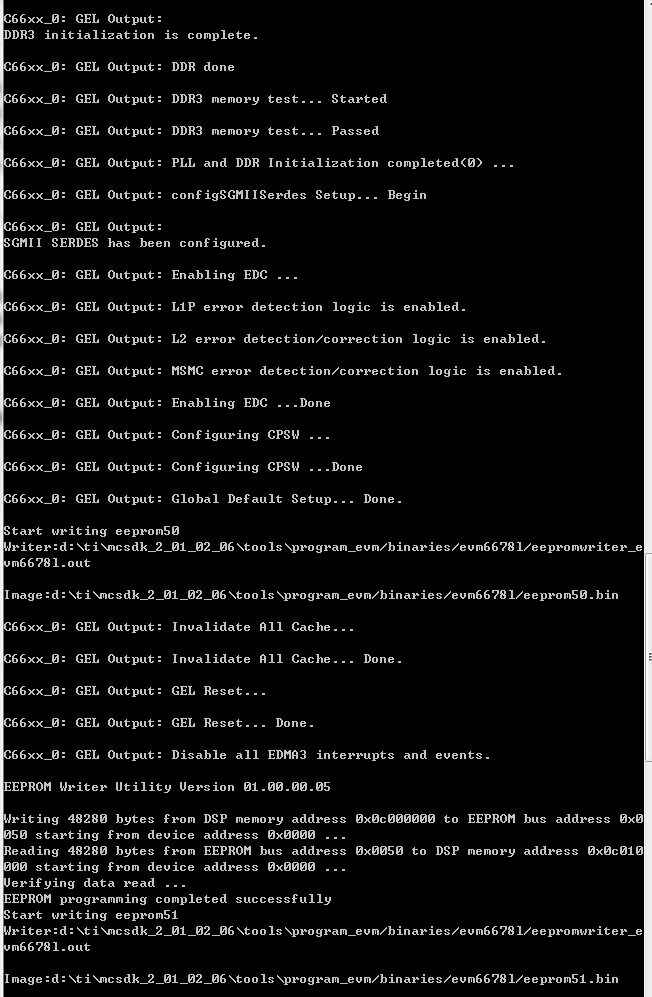
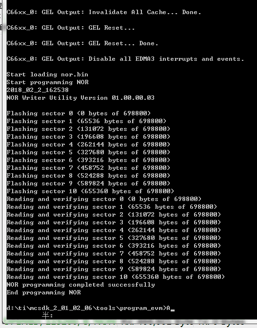
but when i do the Varification as shown in page 14 of program_evm_userguide,the UART didn't print the information described in the doc,but it print some garbled characters like this:

i didn't know what's going on,and when i do the Verifying NOR it also didn't print information like the doc mentioned.briefly,it seems like the IBL can't start up rightly.i hpoe someone can help me,thanks,sincerely!

  • The team is notified. They will post their feedback directly here.

    BR
    Tsvetolin Shulev
  • Can you please indicate what doc you are following to complete this operation? Are you certain that you are connecting Serial connection at 115.2 Kbps ? I don`t see any error when you are restoring the IBL and the NOR images. Can you also indicate the boot Switch settings that you used when you restarted the EVM after programming the EEPROM?
  • thanks for your reply.I do the operation following "d:\ti\mcsdk_2_01_02_06\tools\program_evm\program_evm_userguide.pdf",yes,i connect serial port at 115200,the boot Switch settings is set as the doc described,when i verify POST ,i Set the dip switches as the following

    and do the next operations following this

    but the print information is not right,so i don't know the IBL is start up rightly or not

  • After the boot fails, can you please connect a JTAG emulator and run the Debug GEL file. This will indicate if the boot completed successuly, check for error code and indicate the Program counter at which the DSP is executing code.
    processors.wiki.ti.com/.../Keystone_Device_Architecture

    In CCS run the GEL from Scripts menu and attach the fail log on this E2E for us to analyze.

    Regards,
    Rahul
  • Hi,I connect a JTAG  emulator and run the Debug GEL file(Shannon_SystemDebug_v0.4.gel,6678),and then connect core0,in the "Scripts"menu,there are lots of choices,I click the"C6678_Boot_Status",and here is the output

    C66xx_0: GEL Output: *******************************************************************************************************
    C66xx_0: GEL Output: ********************************** C6678 BOOTSTRAP CONFIGURATION ******************************************************
    C66xx_0: GEL Output: *******************************************************************************************************

    C66xx_0: GEL Output: ********************************** C6678 Device Status Register (DEVSTAT) ************************************

    C66xx_0: GEL Output: BOOTCFG_DEVSTAT ---> 0x0001002B

    C66xx_0: GEL Output: LENDIAN[0] ---> Little Endian
    C66xx_0: GEL Output: BOOTMODE[3:1] ---> I2C Boot Mode
    C66xx_0: GEL Output: SmartReflex ID[5:4] ---> 2
    C66xx_0: GEL Output: MODE[10] ---> Master Mode
    C66xx_0: GEL Output: ADDRESS[11] ---> Boot From I2C EEPROM at I2C bus address 0x50
    C66xx_0: GEL Output: SPEED[12] ---> I2C data rate set to approximately 20 kHz
    C66xx_0: GEL Output: PARAMETER IDX[9:4] ---> 2
    C66xx_0: GEL Output: PCIESSEN[16] ---> Initial state of the power domain and the clock domain for PCIE subsystem is Enabled
    C66xx_0: GEL Output: PCIESSMODE[15:14] ---> PCIE in End-point mode
    C66xx_0: GEL Output: PASSCLKSEL[17] ---> SYSCLK / ALTCORECLK (controlled by CORECLKSEL pin) is used as the input to PA_SS PLL
    C66xx_0: GEL Output: SYSCLKOUTEN[0] ---> No Clock Output

    C66xx_0: GEL Output: ********************************** C6678 DIEID Register (DIEID) ************************************

    C66xx_0: GEL Output: DIEID0 ---> 0x1400F011
    C66xx_0: GEL Output: DIEID1 ---> 0x0403E917
    C66xx_0: GEL Output: DIEID2 ---> 0x00000000
    C66xx_0: GEL Output: DIEID3 ---> 0x313A0001
    C66xx_0: GEL Output: ********************************** C6678 MACID Register (MACID) ************************************

    C66xx_0: GEL Output: MACID[31:0] ---> 0xEAD06FE4
    C66xx_0: GEL Output: MACID[32:47] ---> 0x0017
    C66xx_0: GEL Output: BCAST[16](Broadcast Reception) ---> Broadcast
    C66xx_0: GEL Output: BCAST[17](MAC Flow Control) ---> Off
    C66xx_0: GEL Output: CHECKSUM[24:31] ---> 0xAD

    C66xx_0: GEL Output: *******************************************************************************************************
    C66xx_0: GEL Output: ********************************** C6678 BOOT STATUS ******************************************************
    C66xx_0: GEL Output: *******************************************************************************************************

    C66xx_0: GEL Output: BOOTPROGRESS[31:0] ---> 0x28000100
    C66xx_0: GEL Output: BOOTCFG_BOOTCOMPLETE ---> 0x00000001

    C66xx_0: GEL Output: C6678 Core 0 ---> Boot process Completed
    C66xx_0: GEL Output: C6678 Core 1 ---> Boot in process. Not Complete
    C66xx_0: GEL Output: C6678 Core 2 ---> Boot in process. Not Complete
    C66xx_0: GEL Output: C6678 Core 3 ---> Boot in process. Not Complete
    C66xx_0: GEL Output: C6678 Core 4 ---> Boot in process. Not Complete
    C66xx_0: GEL Output: C6678 Core 5 ---> Boot in process. Not Complete
    C66xx_0: GEL Output: C6678 Core 6 ---> Boot in process. Not Complete
    C66xx_0: GEL Output: C6678 Core 7 ---> Boot in process. Not Complete

    as for the PC value, I dont know where to find it,I wonder if it is in memory browser,but I dont know the PC adress

    Thanks.

  • and here is Device_Config_State_Snapshot,I hope it will help you analysis

    C66xx_0: GEL Output: *******************************************************************************************************
    C66xx_0: GEL Output: ********************************** C6678 BOOTSTRAP CONFIGURATION ******************************************************
    C66xx_0: GEL Output: *******************************************************************************************************

    C66xx_0: GEL Output: ********************************** C6678 Device Status Register (DEVSTAT) ************************************

    C66xx_0: GEL Output: BOOTCFG_DEVSTAT ---> 0x0001002B

    C66xx_0: GEL Output: LENDIAN[0] ---> Little Endian
    C66xx_0: GEL Output: BOOTMODE[3:1] ---> I2C Boot Mode
    C66xx_0: GEL Output: SmartReflex ID[5:4] ---> 2
    C66xx_0: GEL Output: MODE[10] ---> Master Mode
    C66xx_0: GEL Output: ADDRESS[11] ---> Boot From I2C EEPROM at I2C bus address 0x50
    C66xx_0: GEL Output: SPEED[12] ---> I2C data rate set to approximately 20 kHz
    C66xx_0: GEL Output: PARAMETER IDX[9:4] ---> 2
    C66xx_0: GEL Output: PCIESSEN[16] ---> Initial state of the power domain and the clock domain for PCIE subsystem is Enabled
    C66xx_0: GEL Output: PCIESSMODE[15:14] ---> PCIE in End-point mode
    C66xx_0: GEL Output: PASSCLKSEL[17] ---> SYSCLK / ALTCORECLK (controlled by CORECLKSEL pin) is used as the input to PA_SS PLL
    C66xx_0: GEL Output: SYSCLKOUTEN[0] ---> No Clock Output

    C66xx_0: GEL Output: ********************************** C6678 DIEID Register (DIEID) ************************************

    C66xx_0: GEL Output: DIEID0 ---> 0x1400F011
    C66xx_0: GEL Output: DIEID1 ---> 0x0403E917
    C66xx_0: GEL Output: DIEID2 ---> 0x00000000
    C66xx_0: GEL Output: DIEID3 ---> 0x313A0001
    C66xx_0: GEL Output: ********************************** C6678 MACID Register (MACID) ************************************

    C66xx_0: GEL Output: MACID[31:0] ---> 0xEAD06FE4
    C66xx_0: GEL Output: MACID[32:47] ---> 0x0017
    C66xx_0: GEL Output: BCAST[16](Broadcast Reception) ---> Broadcast
    C66xx_0: GEL Output: BCAST[17](MAC Flow Control) ---> Off
    C66xx_0: GEL Output: CHECKSUM[24:31] ---> 0xAD

    C66xx_0: GEL Output: *******************************************************************************************************
    C66xx_0: GEL Output: ********************************** C6678 MASTER VBUSM PRIORITY CONFIGURATION **********************************
    C66xx_0: GEL Output: ************************************PRIORITY-0 (Highest) & PRIORITY-7 (Lowest)********************************

    C66xx_0: GEL Output: EDMA0_TC0 Master: Priority-0
    C66xx_0: GEL Output: EDMA0_TC1 Master: Priority-0

    C66xx_0: GEL Output: EDMA1_TC0 Master: Priority-0
    C66xx_0: GEL Output: EDMA1_TC1 Master: Priority-0
    C66xx_0: GEL Output: EDMA1_TC2 Master: Priority-0
    C66xx_0: GEL Output: EDMA1_TC3 Master: Priority-0

    C66xx_0: GEL Output: EDMA2_TC0 Master: Priority-0
    C66xx_0: GEL Output: EDMA2_TC1 Master: Priority-0
    C66xx_0: GEL Output: EDMA2_TC2 Master: Priority-0
    C66xx_0: GEL Output: EDMA2_TC3 Master: Priority-0

    C66xx_0: GEL Output: PA PKT DMA Master: TX Priority-0, RX Priority-0

    C66xx_0: GEL Output: SRIO PKT DMA Master: TX Priority-0, RX Priority-0

    C66xx_0: GEL Output: QMSS PKT DMA Master: TX Priority-0, RX Priority-0

    C66xx_0: GEL Output: QM_Second Master: Priority-0

    C66xx_0: GEL Output: SRIO Master: Priority-0

    C66xx_0: GEL Output: PCIE Master: Priority-0

    C66xx_0: GEL Output: HYPERBRIDGE Master: Priority at VBUSM is determined according to the priority field value
    C66xx_0: GEL Output: received from the command word. The pri bit encoding is given below:
    C66xx_0: GEL Output: pri-0b0 ---> Priority0 on the VBUSM
    C66xx_0: GEL Output: pri-0b1 ---> Priority4 on the VBUSM

    C66xx_0: GEL Output: COREPAC0 MDMA Master(For other COREPACs load the GEL on the respective COREPAC): Urgent Priority-6, Normal Priority-7

    C66xx_0: GEL Output: *************************** Voltage Control Identification Register (VCNTLID) ****************************

    C66xx_0: GEL Output: PSC_VCNTLID ---> 0x0FFF0000

    C66xx_0: GEL Output: SmartReflex Class-0 VCNTL selection coming from EFUSE(VCNTL) ---> 63
    C66xx_0: GEL Output: Vdd corresponding to VCNTL#63: 1.103 Volts

    C66xx_0: GEL Output: *******************************************************************************************************
    C66xx_0: GEL Output: ********************************** C6678 PSC PWR DOMAINS STATUS **************************************
    C66xx_0: GEL Output: *******************************************************************************************************

    C66xx_0: GEL Output: Most peripheral logic (pwr domain) is in ##0N## state
    C66xx_0: GEL Output: Per-core TETB and System TETB (pwr domain) is in **OFF** state
    C66xx_0: GEL Output: Packet Coprocessor (pwr domain) is in **OFF** state
    C66xx_0: GEL Output: PCIe (pwr domain) is in ##0N## state
    C66xx_0: GEL Output: SRIO (pwr domain) is in **OFF** state
    C66xx_0: GEL Output: HyperLink (pwr domain) is in **OFF** state
    C66xx_0: GEL Output: MSMC RAM (pwr domain) is in ##0N## state
    C66xx_0: GEL Output: C66x Core 0, L1/L2 RAMs (pwr domain) is in ##0N## state
    C66xx_0: GEL Output: C66x Core 1, L1/L2 RAMs (pwr domain) is in ##0N## state
    C66xx_0: GEL Output: C66x Core 2, L1/L2 RAMs (pwr domain) is in ##0N## state
    C66xx_0: GEL Output: C66x Core 3, L1/L2 RAMs (pwr domain) is in ##0N## state
    C66xx_0: GEL Output: C66x Core 4, L1/L2 RAMs (pwr domain) is in ##0N## state
    C66xx_0: GEL Output: C66x Core 5, L1/L2 RAMs (pwr domain) is in ##0N## state
    C66xx_0: GEL Output: C66x Core 6, L1/L2 RAMs (pwr domain) is in ##0N## state
    C66xx_0: GEL Output: C66x Core 7, L1/L2 RAMs (pwr domain) is in ##0N## state
    C66xx_0: GEL Output: *******************************************************************************************************
    C66xx_0: GEL Output: ********************************** C6678 PSC CLOCK DOMAINS STATUS **************************************
    C66xx_0: GEL Output: *******************************************************************************************************

    C66xx_0: GEL Output: SHARED LPSC for all peripherals Clock domain Status:

    C66xx_0: GEL Output: STATE[5:0] ---> ##Enable## state
    C66xx_0: GEL Output: MRST[10] ---> Module reset is ##de-asserted##
    C66xx_0: GEL Output: MRSTDONE[11] ---> Module reset is ##done##
    C66xx_0: GEL Output: MCKOUT[12] ---> Module clock is ##ON##

    C66xx_0: GEL Output: SmartReflex Clock domain Status:

    C66xx_0: GEL Output: STATE[5:0] ---> ##Enable## state
    C66xx_0: GEL Output: MRST[10] ---> Module reset is ##de-asserted##
    C66xx_0: GEL Output: MRSTDONE[11] ---> Module reset is ##done##
    C66xx_0: GEL Output: MCKOUT[12] ---> Module clock is ##ON##

    C66xx_0: GEL Output: DDR3 EMIF Clock domain Status:

    C66xx_0: GEL Output: STATE[5:0] ---> ##Enable## state
    C66xx_0: GEL Output: MRST[10] ---> Module reset is ##de-asserted##
    C66xx_0: GEL Output: MRSTDONE[11] ---> Module reset is ##done##
    C66xx_0: GEL Output: MCKOUT[12] ---> Module clock is ##ON##

    C66xx_0: GEL Output: RESETISO[12] ---> RESET ISOLATION is ##Enabled##

    C66xx_0: GEL Output: EMIF16-SPI Clock domain Status:

    C66xx_0: GEL Output: STATE[5:0] ---> ##Enable## state
    C66xx_0: GEL Output: MRST[10] ---> Module reset is ##de-asserted##
    C66xx_0: GEL Output: MRSTDONE[11] ---> Module reset is ##done##
    C66xx_0: GEL Output: MCKOUT[12] ---> Module clock is ##ON##

    C66xx_0: GEL Output: TSIP Clock domain Status:

    C66xx_0: GEL Output: STATE[5:0] ---> **SwRstDisable** state
    C66xx_0: GEL Output: MRST[10] ---> Module reset is **asserted**
    C66xx_0: GEL Output: MRSTDONE[11] ---> Module reset is ##done##
    C66xx_0: GEL Output: MCKOUT[12] ---> Module clock is **OFF**

    C66xx_0: GEL Output: Debug Subsystem and Tracers Clock domain Status:

    C66xx_0: GEL Output: STATE[5:0] ---> **SwRstDisable** state
    C66xx_0: GEL Output: MRST[10] ---> Module reset is **asserted**
    C66xx_0: GEL Output: MRSTDONE[11] ---> Module reset is ##done##
    C66xx_0: GEL Output: MCKOUT[12] ---> Module clock is **OFF**

    C66xx_0: GEL Output: Per-core TETB and System TETB Clock domain Status:

    C66xx_0: GEL Output: STATE[5:0] ---> **SwRstDisable** state
    C66xx_0: GEL Output: MRST[10] ---> Module reset is **asserted**
    C66xx_0: GEL Output: MRSTDONE[11] ---> Module reset is ##done##
    C66xx_0: GEL Output: MCKOUT[12] ---> Module clock is **OFF**

    C66xx_0: GEL Output: RESETISO[12] ---> RESET ISOLATION is ##Enabled##

    C66xx_0: GEL Output: Packet Accelerator Clock domain Status:

    C66xx_0: GEL Output: STATE[5:0] ---> **SwRstDisable** state
    C66xx_0: GEL Output: MRST[10] ---> Module reset is **asserted**
    C66xx_0: GEL Output: MRSTDONE[11] ---> Module reset is ##done##
    C66xx_0: GEL Output: MCKOUT[12] ---> Module clock is **OFF**

    C66xx_0: GEL Output: Ethernet SGMIIs Clock domain Status:

    C66xx_0: GEL Output: STATE[5:0] ---> **SwRstDisable** state
    C66xx_0: GEL Output: MRST[10] ---> Module reset is **asserted**
    C66xx_0: GEL Output: MRSTDONE[11] ---> Module reset is ##done##
    C66xx_0: GEL Output: MCKOUT[12] ---> Module clock is **OFF**

    C66xx_0: GEL Output: RESETISO[12] ---> RESET ISOLATION is ##Enabled##

    C66xx_0: GEL Output: Security Accelerator Clock domain Status:

    C66xx_0: GEL Output: STATE[5:0] ---> **SwRstDisable** state
    C66xx_0: GEL Output: MRST[10] ---> Module reset is **asserted**
    C66xx_0: GEL Output: MRSTDONE[11] ---> Module reset is ##done##
    C66xx_0: GEL Output: MCKOUT[12] ---> Module clock is **OFF**

    C66xx_0: GEL Output: PCIe Clock domain Status:

    C66xx_0: GEL Output: STATE[5:0] ---> ##Enable## state
    C66xx_0: GEL Output: MRST[10] ---> Module reset is ##de-asserted##
    C66xx_0: GEL Output: MRSTDONE[11] ---> Module reset is ##done##
    C66xx_0: GEL Output: MCKOUT[12] ---> Module clock is ##ON##

    C66xx_0: GEL Output: SRIO Clock domain Status:

    C66xx_0: GEL Output: STATE[5:0] ---> **SwRstDisable** state
    C66xx_0: GEL Output: MRST[10] ---> Module reset is **asserted**
    C66xx_0: GEL Output: MRSTDONE[11] ---> Module reset is ##done##
    C66xx_0: GEL Output: MCKOUT[12] ---> Module clock is **OFF**

    C66xx_0: GEL Output: RESETISO[12] ---> RESET ISOLATION is ##Enabled##

    C66xx_0: GEL Output: HyperLink Clock domain Status:

    C66xx_0: GEL Output: STATE[5:0] ---> **SwRstDisable** state
    C66xx_0: GEL Output: MRST[10] ---> Module reset is **asserted**
    C66xx_0: GEL Output: MRSTDONE[11] ---> Module reset is ##done##
    C66xx_0: GEL Output: MCKOUT[12] ---> Module clock is **OFF**

    C66xx_0: GEL Output: MSMC RAM Clock domain Status:

    C66xx_0: GEL Output: STATE[5:0] ---> ##Enable## state
    C66xx_0: GEL Output: MRST[10] ---> Module reset is ##de-asserted##
    C66xx_0: GEL Output: MRSTDONE[11] ---> Module reset is ##done##
    C66xx_0: GEL Output: MCKOUT[12] ---> Module clock is ##ON##

    C66xx_0: GEL Output: C66x Core 0 and Timer 0 Clock domain Status:

    C66xx_0: GEL Output: STATE[5:0] ---> ##Enable## state
    C66xx_0: GEL Output: MRST[8] ---> Local reset is ##de-asserted##
    C66xx_0: GEL Output: LRSTDONE[11] ---> Local reset is ##done##
    C66xx_0: GEL Output: MRST[10] ---> Module reset is ##de-asserted##
    C66xx_0: GEL Output: MRSTDONE[11] ---> Module reset is ##done##
    C66xx_0: GEL Output: MCKOUT[12] ---> Module clock is ##ON##

    C66xx_0: GEL Output: C66x Core 1 and Timer 1 Clock domain Status:

    C66xx_0: GEL Output: STATE[5:0] ---> ##Enable## state
    C66xx_0: GEL Output: MRST[8] ---> Local reset is ##de-asserted##
    C66xx_0: GEL Output: LRSTDONE[11] ---> Local reset is ##done##
    C66xx_0: GEL Output: MRST[10] ---> Module reset is ##de-asserted##
    C66xx_0: GEL Output: MRSTDONE[11] ---> Module reset is ##done##
    C66xx_0: GEL Output: MCKOUT[12] ---> Module clock is ##ON##

    C66xx_0: GEL Output: C66x Core 2 and Timer 2 Clock domain Status:

    C66xx_0: GEL Output: STATE[5:0] ---> ##Enable## state
    C66xx_0: GEL Output: MRST[8] ---> Local reset is ##de-asserted##
    C66xx_0: GEL Output: LRSTDONE[11] ---> Local reset is ##done##
    C66xx_0: GEL Output: MRST[10] ---> Module reset is ##de-asserted##
    C66xx_0: GEL Output: MRSTDONE[11] ---> Module reset is ##done##
    C66xx_0: GEL Output: MCKOUT[12] ---> Module clock is ##ON##

    C66xx_0: GEL Output: C66x Core 3 and Timer 3 Clock domain Status:

    C66xx_0: GEL Output: STATE[5:0] ---> ##Enable## state
    C66xx_0: GEL Output: MRST[8] ---> Local reset is ##de-asserted##
    C66xx_0: GEL Output: LRSTDONE[11] ---> Local reset is ##done##
    C66xx_0: GEL Output: MRST[10] ---> Module reset is ##de-asserted##
    C66xx_0: GEL Output: MRSTDONE[11] ---> Module reset is ##done##
    C66xx_0: GEL Output: MCKOUT[12] ---> Module clock is ##ON##

    C66xx_0: GEL Output: C66x Core 4 and Timer 4 Clock domain Status:

    C66xx_0: GEL Output: STATE[5:0] ---> ##Enable## state
    C66xx_0: GEL Output: MRST[8] ---> Local reset is ##de-asserted##
    C66xx_0: GEL Output: LRSTDONE[11] ---> Local reset is ##done##
    C66xx_0: GEL Output: MRST[10] ---> Module reset is ##de-asserted##
    C66xx_0: GEL Output: MRSTDONE[11] ---> Module reset is ##done##
    C66xx_0: GEL Output: MCKOUT[12] ---> Module clock is ##ON##

    C66xx_0: GEL Output: C66x Core 5 and Timer 5 Clock domain Status:

    C66xx_0: GEL Output: STATE[5:0] ---> ##Enable## state
    C66xx_0: GEL Output: MRST[8] ---> Local reset is ##de-asserted##
    C66xx_0: GEL Output: LRSTDONE[11] ---> Local reset is ##done##
    C66xx_0: GEL Output: MRST[10] ---> Module reset is ##de-asserted##
    C66xx_0: GEL Output: MRSTDONE[11] ---> Module reset is ##done##
    C66xx_0: GEL Output: MCKOUT[12] ---> Module clock is ##ON##

    C66xx_0: GEL Output: C66x Core 6 and Timer 6 Clock domain Status:

    C66xx_0: GEL Output: STATE[5:0] ---> ##Enable## state
    C66xx_0: GEL Output: MRST[8] ---> Local reset is ##de-asserted##
    C66xx_0: GEL Output: LRSTDONE[11] ---> Local reset is ##done##
    C66xx_0: GEL Output: MRST[10] ---> Module reset is ##de-asserted##
    C66xx_0: GEL Output: MRSTDONE[11] ---> Module reset is ##done##
    C66xx_0: GEL Output: MCKOUT[12] ---> Module clock is ##ON##

    C66xx_0: GEL Output: C66x Core 7 and Timer 7 Clock domain Status:

    C66xx_0: GEL Output: STATE[5:0] ---> ##Enable## state
    C66xx_0: GEL Output: MRST[8] ---> Local reset is ##de-asserted##
    C66xx_0: GEL Output: LRSTDONE[11] ---> Local reset is ##done##
    C66xx_0: GEL Output: MRST[10] ---> Module reset is ##de-asserted##
    C66xx_0: GEL Output: MRSTDONE[11] ---> Module reset is ##done##
    C66xx_0: GEL Output: MCKOUT[12] ---> Module clock is ##ON##

    C66xx_0: GEL Output: *******************************************************************************************************
    C66xx_0: GEL Output: ********************************** C6678 BOOT STATUS ******************************************************
    C66xx_0: GEL Output: *******************************************************************************************************

    C66xx_0: GEL Output: BOOTPROGRESS[31:0] ---> 0x28000100
    C66xx_0: GEL Output: BOOTCFG_BOOTCOMPLETE ---> 0x00000001

    C66xx_0: GEL Output: C6678 Core 0 ---> Boot process Completed
    C66xx_0: GEL Output: C6678 Core 1 ---> Boot in process. Not Complete
    C66xx_0: GEL Output: C6678 Core 2 ---> Boot in process. Not Complete
    C66xx_0: GEL Output: C6678 Core 3 ---> Boot in process. Not Complete
    C66xx_0: GEL Output: C6678 Core 4 ---> Boot in process. Not Complete
    C66xx_0: GEL Output: C6678 Core 5 ---> Boot in process. Not Complete
    C66xx_0: GEL Output: C6678 Core 6 ---> Boot in process. Not Complete
    C66xx_0: GEL Output: C6678 Core 7 ---> Boot in process. Not Complete
    C66xx_0: GEL Output: *******************************************************************************************************
    C66xx_0: GEL Output: ********************************** C6678 RESET STATUS ******************************************************
    C66xx_0: GEL Output: *******************************************************************************************************

    C66xx_0: GEL Output: BOOTCFG_RESET_STAT ---> 0x80000000

    C66xx_0: GEL Output: C6678 Global Reset ---> Device received a global reset
    C66xx_0: GEL Output: C6678 Core 0 Reset ---> Core 0 has not received a local reset
    C66xx_0: GEL Output: C6678 Core 1 Reset ---> Core 1 has not received a local reset
    C66xx_0: GEL Output: C6678 Core 2 Reset ---> Core 2 has not received a local reset
    C66xx_0: GEL Output: C6678 Core 3 Reset ---> Core 3 has not received a local reset
    C66xx_0: GEL Output: C6678 Core 4 Reset ---> Core 4 has not received a local reset
    C66xx_0: GEL Output: C6678 Core 5 Reset ---> Core 5 has not received a local reset
    C66xx_0: GEL Output: C6678 Core 6 Reset ---> Core 6 has not received a local reset
    C66xx_0: GEL Output: C6678 Core 7 Reset ---> Core 7 has not received a local reset
    C66xx_0: GEL Output: *******************************************************************************************************
    C66xx_0: GEL Output: ********************************** C6678 EFUSE AUTOLOAD STATUS ******************************************************
    C66xx_0: GEL Output: *******************************************************************************************************

    C66xx_0: GEL Output: PLLCONTROL_FUSE_ERR ---> 0x00000000

    C66xx_0: GEL Output: Efuse Autoload ##PASS##
    C66xx_0: GEL Output: *******************************************************************************************************
    C66xx_0: GEL Output: ********************************** C6678 MAIN PLL CONFIGURATION ******************************************************
    C66xx_0: GEL Output: *******************************************************************************************************

    C66xx_0: GEL Output: BOOTCFG_MAINPLLCTL0 ---> 0x09000000
    C66xx_0: GEL Output: BOOTCFG_MAINPLLCTL1 ---> 0x00000040

    C66xx_0: GEL Output: PLLD : 0
    C66xx_0: GEL Output: PLLM[12:6] : 0
    C66xx_0: GEL Output: BYPASS : 0
    C66xx_0: GEL Output: BWADJ[7:0] : 9
    C66xx_0: GEL Output: BWADJ[11:8] : 0
    C66xx_0: GEL Output: *******************************************************************************************************
    C66xx_0: GEL Output: ********************************** PLL CONTROLLER CONFIGURATION SNAPSHOT **************************************
    C66xx_0: GEL Output: *******************************************************************************************************

    C66xx_0: GEL Output: *************************** PLL Control Register (PLLCTL) ****************************

    C66xx_0: GEL Output: PLLCONTROL_PLLCTL ---> 0x00000041

    C66xx_0: GEL Output: PLLEN[0] ---> PLL mode. Dividers PREDIV and PLL are ##not bypassed##
    C66xx_0: GEL Output: PLLPWRDN[1] ---> PLL is ##operational##
    C66xx_0: GEL Output: PLLRST[3] ---> PLL reset is ##released##
    C66xx_0: GEL Output: PLLENSRC[5] ---> PLLEN bit is ##enabled##

    C66xx_0: GEL Output: *************************** PLL Multiplier Control Register (PLLM) ****************************

    C66xx_0: GEL Output: PLLCONTROL_PLLM ---> 0x00000013

    C66xx_0: GEL Output: PLLM[5:0] ---> 19 multiplier rate

    C66xx_0: GEL Output: *************************** PLL Pre-Divider Registers (PREDIV) ****************************

    C66xx_0: GEL Output: PLLCONTROL_PREDIV ---> 0x00000000

    C66xx_0: GEL Output: RATIO[4:0] ---> /1. Divide frequency by 1
    C66xx_0: GEL Output: PREDEN[15] ---> Pre-divider is **disabled**. No clock output

    C66xx_0: GEL Output: *************************** PLL Controller Divider Register (PLLDIV1) ****************************

    C66xx_0: GEL Output: PLLCONTROL_PLLDIV1 ---> 0x00008000
    C66xx_0: GEL Output: RATIO[4:0] ---> /1. Divide frequency by 1
    C66xx_0: GEL Output: D1EN[15] ---> Divider1 is ##enabled##
    C66xx_0: GEL Output: *************************** PLL Controller Divider Register (PLLDIV2) ****************************

    C66xx_0: GEL Output: PLLCONTROL_PLLDIV2 ---> 0x00008002
    C66xx_0: GEL Output: RATIO[4:0] ---> /3. Divide frequency by 3
    C66xx_0: GEL Output: D2EN[15] ---> Divider2 is ##enabled##
    C66xx_0: GEL Output: *************************** PLL Controller Divider Register (PLLDIV3) ****************************

    C66xx_0: GEL Output: PLLCONTROL_PLLDIV3 ---> 0x00008001
    C66xx_0: GEL Output: RATIO[4:0] ---> /2. Divide frequency by 2
    C66xx_0: GEL Output: D3EN[15] ---> Divider3 is ##enabled##
    C66xx_0: GEL Output: *************************** PLL Controller Divider Register (PLLDIV4) ****************************

    C66xx_0: GEL Output: PLLCONTROL_PLLDIV4 ---> 0x00008002
    C66xx_0: GEL Output: RATIO[4:0] ---> /3. Divide frequency by 3
    C66xx_0: GEL Output: D4EN[15] ---> Divider4 is ##enabled##
    C66xx_0: GEL Output: *************************** PLL Controller Divider Register (PLLDIV5) ****************************

    C66xx_0: GEL Output: PLLCONTROL_PLLDIV5 ---> 0x00008004
    C66xx_0: GEL Output: RATIO[4:0] ---> /5. Divide frequency by 5
    C66xx_0: GEL Output: D5EN[15] ---> Divider5 is ##enabled##
    C66xx_0: GEL Output: *************************** PLL Controller Divider Register (PLLDIV6) ****************************

    C66xx_0: GEL Output: PLLCONTROL_PLLDIV6 ---> 0x0000803F
    C66xx_0: GEL Output: RATIO[4:0] ---> /64. Divide frequency by 64
    C66xx_0: GEL Output: D6EN[15] ---> Divider6 is ##enabled##
    C66xx_0: GEL Output: *************************** PLL Controller Divider Register (PLLDIV7) ****************************

    C66xx_0: GEL Output: PLLCONTROL_PLLDIV7 ---> 0x00008005
    C66xx_0: GEL Output: RATIO[4:0] ---> /6. Divide frequency by 6
    C66xx_0: GEL Output: D7EN[15] ---> Divider7 is ##enabled##
    C66xx_0: GEL Output: *************************** PLL Controller Divider Register (PLLDIV8) ****************************

    C66xx_0: GEL Output: PLLCONTROL_PLLDIV8 ---> 0x0000803F
    C66xx_0: GEL Output: RATIO[4:0] ---> /64. Divide frequency by 64
    C66xx_0: GEL Output: D8EN[15] ---> Divider8 is ##enabled##
    C66xx_0: GEL Output: *************************** PLL Controller Divider Register (PLLDIV9) ****************************

    C66xx_0: GEL Output: PLLCONTROL_PLLDIV9 ---> 0x0000800B
    C66xx_0: GEL Output: RATIO[4:0] ---> /12. Divide frequency by 12
    C66xx_0: GEL Output: D9EN[15] ---> Divider9 is ##enabled##
    C66xx_0: GEL Output: *************************** PLL Controller Divider Register (PLLDIV10) ****************************

    C66xx_0: GEL Output: PLLCONTROL_PLLDIV10 ---> 0x00008002
    C66xx_0: GEL Output: RATIO[4:0] ---> /3. Divide frequency by 3
    C66xx_0: GEL Output: D10EN[15] ---> Divider10 is ##enabled##
    C66xx_0: GEL Output: *************************** PLL Controller Divider Register (PLLDIV11) ****************************

    C66xx_0: GEL Output: PLLCONTROL_PLLDIV11 ---> 0x00008005
    C66xx_0: GEL Output: RATIO[4:0] ---> /6. Divide frequency by 6
    C66xx_0: GEL Output: D11EN[15] ---> Divider11 is ##enabled##
    C66xx_0: GEL Output: *************************** PLL Controller Divider Register (PLLDIV12) ****************************

    C66xx_0: GEL Output: PLLCONTROL_PLLDIV12 ---> 0x00008003
    C66xx_0: GEL Output: RATIO[4:0] ---> /4. Divide frequency by 4
    C66xx_0: GEL Output: D12EN[15] ---> Divider12 is ##enabled##
    C66xx_0: GEL Output: *************************** PLL Controller Divider Register (PLLDIV13) ****************************

    C66xx_0: GEL Output: PLLCONTROL_PLLDIV13 ---> 0x00008007
    C66xx_0: GEL Output: RATIO[4:0] ---> /8. Divide frequency by 8
    C66xx_0: GEL Output: D13EN[15] ---> Divider13 is ##enabled##
    C66xx_0: GEL Output: *************************** PLL Controller Divider Register (PLLDIV14) ****************************

    C66xx_0: GEL Output: PLLCONTROL_PLLDIV14 ---> 0x00000000
    C66xx_0: GEL Output: RATIO[4:0] ---> /1. Divide frequency by 1
    C66xx_0: GEL Output: D14EN[15] ---> Divider14 is **disabled**. No clock output
    C66xx_0: GEL Output: *************************** PLL Controller Divider Register (PLLDIV15) ****************************

    C66xx_0: GEL Output: PLLCONTROL_PLLDIV15 ---> 0x00000000
    C66xx_0: GEL Output: RATIO[4:0] ---> /1. Divide frequency by 1
    C66xx_0: GEL Output: D15EN[15] ---> Divider15 is **disabled**. No clock output
    C66xx_0: GEL Output: *************************** PLL Controller Divider Register (PLLDIV16) ****************************

    C66xx_0: GEL Output: PLLCONTROL_PLLDIV16 ---> 0x00000000
    C66xx_0: GEL Output: RATIO[4:0] ---> /1. Divide frequency by 1
    C66xx_0: GEL Output: D16EN[15] ---> Divider16 is **disabled**. No clock output

    C66xx_0: GEL Output: *************************** Clock Enable Control Register (CKEN) ****************************

    C66xx_0: GEL Output: PLLCONTROL_CKEN ---> 0x00000000

    C66xx_0: GEL Output: AUXEN[0] ---> **Disable** AUXCLK

    C66xx_0: GEL Output: *************************** Reset Control Register (RSTCTRL) ****************************

    C66xx_0: GEL Output: PLLCONTROL_RSCTRL ---> 0x00010003

    C66xx_0: GEL Output: SWRST[16] ---> Software reset is ##not asserted##

    C66xx_0: GEL Output: *************************** Reset Configuration Register (RSTCFG) ****************************

    C66xx_0: GEL Output: PLLCONTROL_RSCFG ---> 0x00000000

    C66xx_0: GEL Output: WDTYPE[1](Core0 Watchdog Timer initiates a reset of type) ---> Hard Reset (default)
    C66xx_0: GEL Output: WDTYPE[2](Core1 Watchdog Timer initiates a reset of type) ---> Hard Reset (default)
    C66xx_0: GEL Output: WDTYPE[3](Core2 Watchdog Timer initiates a reset of type) ---> Hard Reset (default)
    C66xx_0: GEL Output: WDTYPE[4](Core3 Watchdog Timer initiates a reset of type) ---> Hard Reset (default)
    C66xx_0: GEL Output: RESET(bar)TYPE[12] (RESET(bar)initiated Reset) ---> Hard Reset (default)
    C66xx_0: GEL Output: PLLCTLRSTTYPE[13] ( PLL controller initiated Reset) ---> Hard Reset (default)

    C66xx_0: GEL Output: *************************** Reset Isolation Register (RSISO) ****************************

    C66xx_0: GEL Output: PLLCONTROL_RSISO ---> 0x00000000

    C66xx_0: GEL Output: MOD_ISO[3] ---> AIF2 **Not** reset isolated
    C66xx_0: GEL Output: MOD_ISO[8] ---> Smart-Reflex(SR) **Not** reset isolated
    C66xx_0: GEL Output: MOD_ISO[9] ---> SRIO **Not** reset isolated

    C66xx_0: GEL Output: *************************** PLL Post-Divider Control Register (POSTDIV) ****************************

    C66xx_0: GEL Output: PLLCONTROL_POSTDIV ---> 0x00000000

    C66xx_0: GEL Output: RATIO[4:0] ---> /1. Divide frequency by 1
    C66xx_0: GEL Output: PREDEN[15] ---> Post-divider is **disabled**. No clock output

    C66xx_0: GEL Output: *************************** PLL Secondary Control Register (SECCTL) ****************************

    C66xx_0: GEL Output: PLLCONTROL_SECCTL ---> 0x00090000

    C66xx_0: GEL Output: OUTPUT_DIVIDE[22:19] ---> /2. Divide frequency by 2
    C66xx_0: GEL Output: BYPASS[23] ---> Main PLL Bypass ##disabled##

    C66xx_0: GEL Output: *******************************************************************************************************
    C66xx_0: GEL Output: ********************************** PLL CONTROLLER STATUS SNAPSHOT **************************************
    C66xx_0: GEL Output: *******************************************************************************************************

    C66xx_0: GEL Output: *************************** Clock Status Register (CKSTAT) ****************************

    C66xx_0: GEL Output: PLLCONTROL_CKSTAT ---> 0x00000000

    C66xx_0: GEL Output: AUXON[0] ---> AUXCLK is **gated**

    C66xx_0: GEL Output: *************************** SYSCLK Status Register (SYSTAT) ****************************

    C66xx_0: GEL Output: PLLCONTROL_SYSTAT ---> 0x00001FFF

    C66xx_0: GEL Output: SYS[1]ON ---> SYSCLK1 is ##on##
    C66xx_0: GEL Output: SYS[2]ON ---> SYSCLK2 is ##on##
    C66xx_0: GEL Output: SYS[3]ON ---> SYSCLK3 is ##on##
    C66xx_0: GEL Output: SYS[4]ON ---> SYSCLK4 is ##on##
    C66xx_0: GEL Output: SYS[5]ON ---> SYSCLK5 is ##on##
    C66xx_0: GEL Output: SYS[6]ON ---> SYSCLK6 is ##on##
    C66xx_0: GEL Output: SYS[7]ON ---> SYSCLK7 is ##on##
    C66xx_0: GEL Output: SYS[8]ON ---> SYSCLK8 is ##on##
    C66xx_0: GEL Output: SYS[9]ON ---> SYSCLK9 is ##on##
    C66xx_0: GEL Output: SYS[10]ON ---> SYSCLK10 is ##on##
    C66xx_0: GEL Output: SYS[11]ON ---> SYSCLK11 is ##on##
    C66xx_0: GEL Output: SYS[12]ON ---> SYSCLK12 is ##on##

    C66xx_0: GEL Output: *************************** Reset Type Status Register (RSTYPE) ****************************

    C66xx_0: GEL Output: PLLCONTROL_RSTYPE ---> 0x00000001

    C66xx_0: GEL Output: POR[0] ---> Power-on reset **was** the last reset to occur
    C66xx_0: GEL Output: RESET(bar)[1] ---> RESET(bar)initiated Reset ##was not## the last reset to occur
    C66xx_0: GEL Output: PLLCTLRST[2] ---> PLLCTL initiated Reset ##was not## the last reset to occur
    C66xx_0: GEL Output: WDRST[1] ---> Core0 watchdog Timer initiated Reset ##was not## the last reset to occur
    C66xx_0: GEL Output: WDRST[2] ---> Core1 watchdog Timer initiated Reset ##was not## the last reset to occur
    C66xx_0: GEL Output: WDRST[3] ---> Core2 watchdog Timer initiated Reset ##was not## the last reset to occur
    C66xx_0: GEL Output: WDRST[4] ---> Core3 watchdog Timer initiated Reset ##was not## the last reset to occur
    C66xx_0: GEL Output: EMURST[0] ---> Emulation initiated Reset ##was not## the last reset to occur

    C66xx_0: GEL Output: *******************************************************************************************************
    C66xx_0: GEL Output: ********************************** C6678 BRIDGE SCAN RESULTS ******************************************************
    C66xx_0: GEL Output: *******************************************************************************************************

    C66xx_0: GEL Output: Bridge5 scan Test PASSED
    C66xx_0: GEL Output: Bridge6 scan Test PASSED
    C66xx_0: GEL Output: Bridge7 scan Test PASSED
    C66xx_0: GEL Output: Bridge8 scan Test PASSED
    C66xx_0: GEL Output: Bridge9 scan Test PASSED
    C66xx_0: GEL Output: Bridge10 scan Test PASSED
    C66xx_0: GEL Output: Bridge2 scan Test PASSED
    C66xx_0: GEL Output: Bridge3 scan Test PASSED
    C66xx_0: GEL Output: No Errors detected in the bridge scan

    C66xx_0: GEL Output: BRIDGES NOT TESTED: Bridge1 and Bridge4

    C66xx_0: GEL Output: *******************************************************************************************************
    C66xx_0: GEL Output: ********************************** C6678 SLAVE SCAN RESULTS ******************************************************
    C66xx_0: GEL Output: *******************************************************************************************************

    C66xx_0: GEL Output: SPI Slave scan Test PASSED
    C66xx_0: GEL Output: BOOT_ROM Slave scan Test PASSED
    C66xx_0: GEL Output: COREPAC0 Slave scan Test PASSED
    C66xx_0: GEL Output: COREPAC1 Slave scan Test PASSED
    C66xx_0: GEL Output: COREPAC2 Slave scan Test PASSED
    C66xx_0: GEL Output: COREPAC3 Slave scan Test PASSED
    C66xx_0: GEL Output: COREPAC4 Slave scan Test PASSED
    C66xx_0: GEL Output: COREPAC5 Slave scan Test PASSED
    C66xx_0: GEL Output: COREPAC6 Slave scan Test PASSED
    C66xx_0: GEL Output: COREPAC7 Slave scan Test PASSED
    C66xx_0: GEL Output: MSMC_SMS Slave scan Test PASSED
    C66xx_0: GEL Output: Problem(MSMC_SES STALLED): The MSMC SES slave on SCR_3A is stalled.
    C66xx_0: GEL Output: Reason & Solution: 1) The MSMC module might not be enabled in the Power-Sleep Controller
    C66xx_0: GEL Output: 2) MSMC SES is not responding to reads from Masters on the SCR
    C66xx_0: GEL Output: 3) DDR might not be enabled

    C66xx_0: GEL Output: SLAVES NOT TESTED: SRIO_Slave, PCIe_Slave, HYPERBRIDGE_Slave, QMSS_Slave

    C66xx_0: GEL Output: *************************** C6678 Silicon Revision (PG 1.0 OR PG 2.0) ****************************

    C66xx_0: GEL Output: MM_REVID[31:0] - 0x00080001

    C66xx_0: GEL Output: Silicon Revision UNKNOWN

    Thanks.

  • Another thing I forgot to say,after I power on ,the 4 LEDs are on,in MCSDK user guide,it says

    "At power on, the DSP starts execution with bootrom which transfers execution to the POST boot program from
    EEPROM using the I2C slave bus address as 0x50. The POST will then run through a sequence of platform tests.
    Upon power on, all the 4 FPGA debug LEDs will be on by default, remain ON for approximately 10 sec, then turn
    OFF if all the tests complete successfully. If any of the tests fails, the LED(s) will blink"

    but my 4 led always on even if after 10 sec,does this mean that the POST failed?