This thread has been locked.

If you have a related question, please click the "Ask a related question" button in the top right corner. The newly created question will be automatically linked to this question.

TDA2xx: ProcessorSDK 3.01 PDK PCIe example/PCIe optimization

Hello,

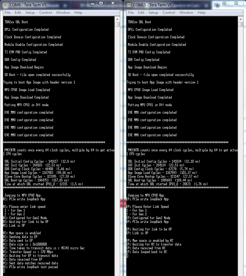
I'm currently trying to optimize PCIe transfers between two TDA2xx's. The test I'm running can be found here: "<PROCESSOR_SDK_ROOT>\ti_components\drivers\pdk_01_08_00_16\packages\ti\csl\example\pcie". One TDA2xx serves as RC and the other one serves as EP. The test sends 16MB of data from RC to EP, data is then looped back from EP to RC where it is compared to the original data. If those are identical the test is successful. System EDMA's are used to perform the transfers.

The test in its current state, without any modifications states that the PCIe throughput is 370 MBps when both RC and EP utilize Gen2 transfer speed.

After reading through some documentation, I found out that, to achieve maximum performance, these requirements need to be met:

1) The EDMA transfer parameters are to be set so that the transfer controller submits the least possible number of transfer requests

2) The EDMA TC default burst size is to be equal to the PCIe payload size

As for the bullet 1), I referred to this table (found in SPRAC21).

In the test, the system EDMA's TC0 is used. I have used EDMA before so I was able to experiment with the (A/B/C)CNT values. For example, the original test which has ACNT=16K, BCNT=16M/16K and CCNT=1 (which do not comply to the table above) gives 370 MBps for throughput. When I set the values to ACNT=128, BCNT=128 and CCNT=1024 (which is recommended in the table) I get 330 MBps which is worse. What else should I try regarding the transfer parameters only?

Regarding bullet 2), that's where I need some clarification.

- I cannot confirm that the EDMA's TC0 is indeed using DBS of 128B which I found to be defined in "<PROCESSOR_SDK_ROOT>\ti_components\drivers\pdk_01_08_00_16\packages\ti\csl\soc\tda2xx\hw_ctrl_core.h" CTRL_CORE_CONTROL_IO_1_TC0_DEFAULT_BURST_SIZE_MASK macro definition. It is not used anywhere and I don't know where to find the code that configures the TC's.

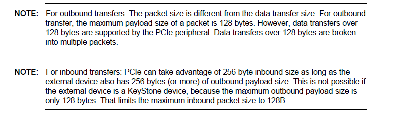
- When we say PCIe payload size, does that mean it is the size of the data being sent in a TLP excluding the headers that are added to it? Also, where can I set the payload size of PCIe's transfers? I suppose that it can be 128B at best which I concluded from this snippet found in SPRABK5B. Both of my devices are KeyStone aren't they (they are TDA2xx)?

I'm currently learning about PCIe and how it works so forgive me for my confusion. I would just like some help optimizing this particular test regarding places in code where all these parameters are set and how to set them correctly.

Sorry for the long post and thank you in advance.

Regards,

Nick

  • Hi Nick,

    TDA2xx is not a Keystone device.

    As far as I know EDMA gives best throughput when ACount=16k, CCount=1, BCount=x.

    Let me find if there is an EDMA configuration which gives better throughput.

    There is lot of documentation freely available online which you can refer to see PCIe packet structure.

    Also the numbers you are seeing are skewed as there are three UART prints in between.

    Can you comment the prints as done below and try:

    //UARTPuts("RC: Link is UP\r\n\r\n", -1);
    
    /*Configure PCIe traffic*/
    PcieAppConfigTrafficRemote();
    /*Wait till mem space is enabled*/
    while (memSpaceEnable != 1U) ;
    //UARTPuts("RC: Mem space is enabled\r\n", -1);
    //UARTPuts("RC: Sending data to EP\r\n", -1);
    /*Init EDMA and enable transfer*/
    PcieAppEdmaInit();

    Regards,

    Rishabh

  • Hi Rishabh,

    actually it is not RC side whose uart prints could skew the numbers because the start time is collected just after configuring EDMA and before triggering the transfer and the end time is collected after RC verifies that data has arrived at EP, there are no uart prints in there. However, EP side does some uart prints while RC is sending the data (and the clock on RC has already started) so if the data sending is really fast then the uart prints at EP could add significant time to the clock.
    However, upon commenting out those prints on the EP side, nothing changed regarding the transfer speed.

    Another thing that I came across is when the start and end times are collected. As I stated above, the start time is collected just before EDMA trigger on RC side which is fine but the end time is collected after verifying that the data arrived at EP. The verification is done by polling a certain value that EP writes in its rx buffer. It is after that the end time is collected. I moved the end time collection before this verification but nothing changed.

    It would be very helpful to me if you could tell me where in code I can set/verify System EDMA TC0's DBS as well as PCIe's payload size.

    Thank you in advance.

    Regards,
    Nick
  • Hi Nick,

    Due to an oversight I had referred to an older version of the example in which start timestamp is at different location.
    The burst size is 128 bytes. Anyway this can be configured by modifying CTRL_CORE_CONTROL_IO_1 register.
    TDA2xx has two PCIe lanes. You can modify PCIE_NUMBER_OF_LANES to 2 to increase the PCIe throughput.
    On TDA2xx max PCIe payload size is 256 bytes which is set upon reset (register PCIECTRL_RC_DBICS_DEV_CAP).

    Regards,
    Rishabh
  • Hi Nick,

    I had discussions regarding EDMA configuration. It seems that EDMA configuration is the most optimal.
    Only optimization possible is having the buffer 128 byte aligned.

    Regards,
    Rishabh
  • Hi Rishabh,

    thank you for the recommendations. I will try them and will get back to you with the results.

    Regards,
    Nick
  • Hi Rishabh,

    Here's what I tried and the corresponding results:

    DONE: declared the dataTxBuffer on RC side as below:
    static volatile uint32_t dataTxBuffer[DATA_SIZE_IN_WORD] __attribute__((aligned(128)));
    RESULT: Nothing changed regarding throughput.

    DONE: enabled 2 lanes in PCIE_NUMBER_OF_LANES
    RESULT: Nothing changed regarding throughput.

    I am currently looking at this document: www.ti.com/.../sprac21.pdf. Table 42 on page 78 is measured performance for pcie operations in X2 GEN2 mode. For WR operation from RC to EP it is stated that measured throughput is 5966.86Mbps which is ~750MBps (for reference I get 370MBps only).
    On page 76 there are configurations with which the performance was measured. The EDMA and PCIe configurations are exactly the same as in the test from PDK so I suppose that test was used when performance was measured. The only configuration that I am not sure is exactly the same for me is timer configuration, could you help me check that?

    Also, I looked into PCIe protocol in more detail and would like to know if the performance measured in the document above is the throughput regarding payload only or the whole packets with 8b/10b encoding that, ultimately, travel through the PCIe link.

    Also, I would be very grateful if you could run the test with one and two lanes and see if there is a difference in measured throughput.

    Thank you in advance.

    Regards,
    Nick

  • Hi Nick,

    The test used for this document is different from the one given in PDK.

    In this document there are two tables. X1 is for single lane and X2 is two lanes.

    With the current system you are able to get 370 MBps for single lane and the document says 3013.15Mbps (376.6 MBps).

    For dual lane the performance should definitely improve (almost twice).

    Can you one again confirm throughput with a clean build for PCIe Gen2 with two lanes.

    Regards,

    Rishabh

  • Hi Rishabh,

    I just installed clean PROCESSOR_SDK_VISION_03_02_00_00, did a clean build of the pdk drivers, sbl and examples. I only changed the NUMBER_OF_LANES macro definition to 2 in pcie_app.h, nothing else. Still no success, it says that throughput is 370MBps.

    Here's the console output from both cores below:


    I have no idea what could be the problem.

    Regards,
    Nick

  • Hi Nick,

    I checked the EVM schematics. It seems that only one PCIe lane is connected on the TDA2xx EVM.
    Hence you cannot establish two lane communication.
    Two lanes numbers in application note were taken by running PCIe test case on Silicon Validation board.
    And the numbers you are getting with single lane are almost the same as the numbers given in performance note.

    Regards,
    Rishabh
  • Hi Rishabh,

    Actually I am testing on a custom board which connects the two SoCs via 2-lane PCIe, I checked our schematics. Are you trying to say that inside the SoC there is only one lane connected to the PCIe subsystem 1, no matter if there are 2 lanes externally connected to the pins?

    Thank you for your help so far.

    Regards,
    Nick

  • Hi Nick,

    SoC supports two lanes. I am talking about TDA2xx EVM which has only one lane connected to the pins.
    In case there are two lanes supported on your board you need to enable the second PHY.
    Can you refer to the board's schematics and make corresponding changes in PCIEAppPrcmConfig().

    Regards,
    Rishabh
  • Hi Rishabh,

    I'm very happy to inform you that I have found what the problem was. Having in mind the hint about PHY you mentioned, I stumbled upon the Table 26-61. PCIePHY Subsystem Low-Level Programming Sequence in TDA2xx TRM (page 7274). There I found two additional steps that were required in order to utilize 2 lanes in PCIe Subsystem 1 that were not present in the original test from PDK. Those are: "Configure the PCIE PHYs to ×1 or ×2 mode", "Configure the PCIESS2 Power Control clock frequency to match SYS_CLK1 in MHz" and "Power up PCIESS2_PHY_TX and PCIESS2_PHY_RX".

    After setting correct values in those registers in the beginning of the PlatformPCIESS1CtrlConfig() function in the pcie_app.c, I am getting steady 740 MBps which is close to the measured value from the TDA2xx performance document.

    The PlatformPCIESS1CtrlConfig() now looks like this:

    void PlatformPCIESS1CtrlConfig(void)
    {
        uint32_t regVal;
    
        /*ENABLE x2 MODE*/
        regVal = HW_RD_REG32(
            SOC_SEC_EFUSE_REGISTERS_BASE + CTRL_CORE_PCIE_CONTROL);
    
        HW_SET_FIELD32(regVal, CTRL_CORE_PCIE_CONTROL_PCIE_B1C0_MODE_SEL,
                        0x01U);
    
        HW_WR_REG32(SOC_SEC_EFUSE_REGISTERS_BASE + CTRL_CORE_PCIE_CONTROL,
                    regVal);
    
        regVal = HW_RD_REG32(
            SOC_SEC_EFUSE_REGISTERS_BASE + CTRL_CORE_PCIE_CONTROL);
    
        HW_SET_FIELD32(regVal, CTRL_CORE_PCIE_CONTROL_PCIE_B0_B1_TSYNCEN,
                        0x01U);
    
        HW_WR_REG32(SOC_SEC_EFUSE_REGISTERS_BASE + CTRL_CORE_PCIE_CONTROL,
                    regVal);
    
        /*CONTROL MODULE PWR CTL REG status of PCIeSS1*/
        regVal = HW_RD_REG32(
            SOC_SEC_EFUSE_REGISTERS_BASE + CTRL_CORE_PHY_POWER_PCIESS1);
    
        HW_SET_FIELD32(regVal, CTRL_CORE_PHY_POWER_PCIESS1_PCIESS1_PWRCTL_CMD,
                        0x03U);
    
        HW_SET_FIELD32(regVal, CTRL_CORE_PHY_POWER_PCIESS1_PCIESS1_PWRCTL_CLKFREQ,
                        0x1AU);
    
        HW_WR_REG32(SOC_SEC_EFUSE_REGISTERS_BASE + CTRL_CORE_PHY_POWER_PCIESS1,
                    regVal);
    
        /*CONTROL MODULE PWR CTL REG status of PCIeSS2*/
        regVal = HW_RD_REG32(
            SOC_SEC_EFUSE_REGISTERS_BASE + CTRL_CORE_PHY_POWER_PCIESS2);
    
        HW_SET_FIELD32(regVal, CTRL_CORE_PHY_POWER_PCIESS2_PCIESS2_PWRCTL_CMD,
                        0x03U);
    
        HW_SET_FIELD32(regVal, CTRL_CORE_PHY_POWER_PCIESS2_PCIESS2_PWRCTL_CLKFREQ,
                        0x1AU);
    
        HW_WR_REG32(SOC_SEC_EFUSE_REGISTERS_BASE + CTRL_CORE_PHY_POWER_PCIESS2,
                    regVal);
    
        /*Set PCIeSS1 delay count*/
        HW_WR_FIELD32(SOC_SEC_EFUSE_REGISTERS_BASE + CTRL_CORE_PCIE_PCS,
                        CTRL_CORE_PCIE_PCS_PCIESS1_PCS_RC_DELAY_COUNT, 0xF1U);
        /*Set PCIeSS2 delay count*/
        HW_WR_FIELD32(SOC_SEC_EFUSE_REGISTERS_BASE + CTRL_CORE_PCIE_PCS,
                        CTRL_CORE_PCIE_PCS_PCIESS2_PCS_RC_DELAY_COUNT, 0xF1U);
    }

    I would like to thank you again for all the help and I hope that people will find this post helpful if they have similar problems.

    Best regards,
    Nick

  • Hi Nick,

    Glad to know that your issue is resolved.
    Thanks for posting a detailed reply for benefit for others.
    Feel free to ask any follow-up questions by creating a new thread.

    Regards,
    Rishabh