This thread has been locked.

If you have a related question, please click the "Ask a related question" button in the top right corner. The newly created question will be automatically linked to this question.

TDA2SG: recommended pcb pad size of TDA2 bga

Part Number: TDA2SG

Hello team,

My customer would like to know if the PCB pad size(land pattern size of BGA) is acceptable.

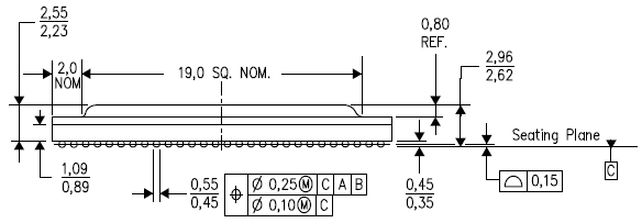
The ball size of TDA2x ABC (23mmx23mm) looks typ. 0.50Φ according to data manual as following.

The customer is designing the PCB pad size with 0.40Φ.  

0.40Φ pad size is acceptable?  .

What would be the recommended pad size for BGA?

regards,

Lloyd

  • Refer to the following appnote for background: www.ti.com/.../spraa99b.pdf

    The solder ball dia that the POD shows is not the key parameter that should be used in determining the PCB’s ball land diameter. The package’s Solder Mask Opening (SMO) for each ball is the parameter that drives PCB ball land dia. Optimally SMO = Ball Land for best mechanical robustness, see Table 1 of attached. It recommends 0.4mm ball land dia for 0.8mm pitch BGAs assuming the standard package side SMO = 0.4mm.

    For TDA2x and DRA74x/75x we recommend 0.4mm ball land dia.

    Regards,
    Kyle