


Part Number: TDA3MA
Hi, all.
The TDA3 TRM says, there is a single CSI2_PHY1 at the CAL_A of the ISS, which is composed of 5 lanes (4 data lanes + 1 clock lane).
1) There is the following configuration register:
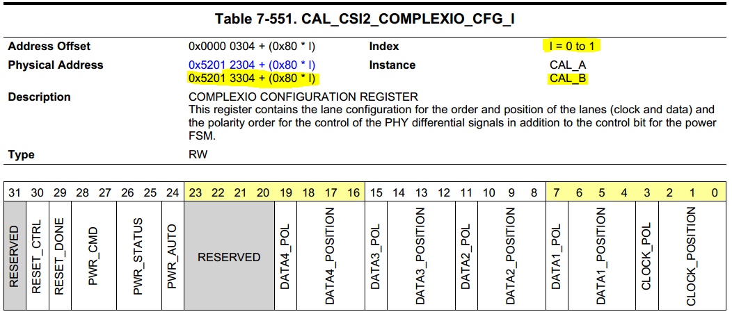
What is the meaning of this register for CAL_B module? If I understand right, there is no any PHY at the CAL_B module.
Except two instances there are 2 available offsets (for I=0 and for I=1), so there are 4 different offsets: 0x52012304, 0x52012384, 0x52013304 and 0x52013384
May you check this issue? What are the purposes of this register at each out of four offsets?
2) The TRM has the following note regarding the clock lane:

However, lets see the description of the clock position bitfield at the previously reminded register:

It has the option to place the clock lane at position 4. So what is true?
Best regards,
Alex

