


Other Parts Discussed in Thread: TMS320C6742
Hi Expert
After long time running, several C6746 SOC exists a bulge phenomenon on prototype before production , after check customer'schematic, we found 2 suspicions, customer want to get confirmation from factory side whether they need change these 2 points, if it really needs, they have to do re-design board.
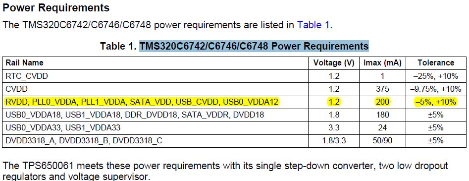
1, In customer design, the pins M2,N4,P1,P2 (SATA_VDD),L15(VDDA12_PLL1),N15(VDDA12_PLL0),M12(USB_CVDD12) is connected to 1.3V, really test result on these power rails is 1.28V~1.3V. According to C6746 datasheet, we know that M2,N4,P1,P2 (SATA_VDD) are reserved pins , and they should be either tied to a STATIC 1.2V supply or left unconnected. But according to slva490.pdf, TMS320C6742/C6746/C6748 Power Requirements, the SATA_VDD has a tolerance from -5%~+10% around1.2V. The test result 1.28V~1.3V should be in the range of -5%~+10%(1.32V), So customer want to know whether 1.3V/1.28V on SATA_VDD is OK and whether could cause possible bulge? The similar questions for L15,N15,M12.
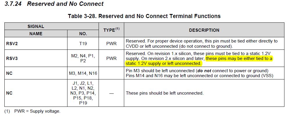
2 The unused pins P14 is connected to 1v8D, P15 is connected to 3v3D, according to datasheet, these 2 pins should be left un-connected, could this possibly cause DSP bulge?
Any suggestions if other possible reason? (C6746 PART Schematic is attached)


