This thread has been locked.

If you have a related question, please click the "Ask a related question" button in the top right corner. The newly created question will be automatically linked to this question.

RTOS/66AK2H14: Invalid magic number in Single image header

Part Number: 66AK2H14

Tool/software: TI-RTOS

Hi,

We have designed  customized  board  using 66AK2H14. We are using CCSV7 and TI XDS 110 debug probe to connect board to CCS.

We are able to Flash MLO and gpio_led application using spi_flashwriter.

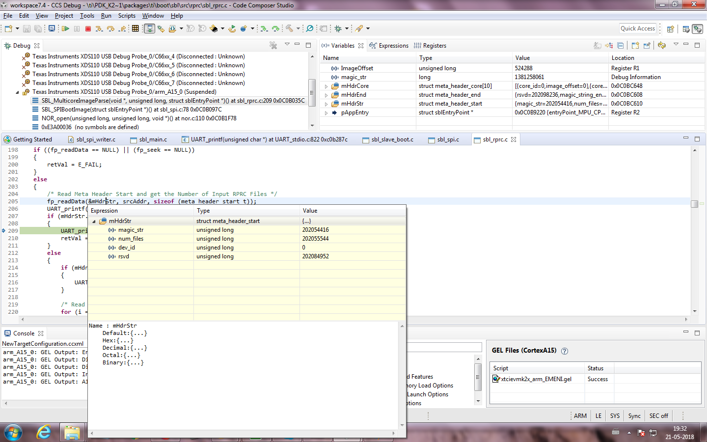
But when boot mode is changed to SPI,  facing below issue:

 
     **** PDK SBL ******
   SBL Revision: 01.00.07.00 (May 18 2018 - 13:05:07)
   Begin parsing user application
   MAGIC NUM: 202084688
   Invalid magic number in Single image header
   Jumping to user application...
 
Flashed same app to EVM , It was running successfully when boot mode is changed to SPI.
Only difference between EVM and custom board binary is MLO. For EVM we used sdk’s prebuilt MLO.
Q1. We just changed DDR3 configuration and Rebuilt MLO through makefile.Is there any other thing we are missing?
Regards,
Mahima Shanbag.

  • The team is notified. They will post their feedback directly here.

    BR
    Tsvetolin Shulev
  • Hi Tsvetolin Shulev,

    I thought issue may be with app header so I checked the app header using hexdump which looks similar to that of pre built post app in C:\ti_new\processor_sdk_rtos_k2hk_4_03_00_05\prebuilt-images.

    I have attached application's header here.

    (200 bytes):
    4D 53 54 52 
    01 00 00 00 
    37 00 00 00 
    00 00 00 00 
    05 00 00 00 
    20 00 00 00 
    00 00 00 00 
    4D 45 4E 44 
    52 50 52 43 
    40 FE 83 00 
    00 00 00 00 
    05 00 00 00 
    01 00 00 00 
    00 20 83 00 
    00 00 00 00 
    40 1D 01 00 
    00 00 00 00 
    00 00 00 00 
    46 23 77 36 
    07 B4 4E 02 
    76 1A 77 95 
    5B A3 04 90 
    30 27 77 86 
    13 0F 01 90 
    27 02 04 80 
    2F 02 E0 E2 
    29 00 00 06 
    C6 B5 77 85 
    D8 1F 98 05 
    52 E0 FF 07 
    05 AC 45 DC 
    D7 82 BF 02 
    10 0A 01 30 
    08 00 40 E2 
    35 EC C7 15 
    AA 12 80 05 
    AA 16 00 05 
    7A 0A AC 20 
    DA 0F 04 21 
    21 21 F8 53 
    A6 36 20 48 
    01 00 20 E0 
    10 AC 1C 70 
    DA 0F A0 42 
    00 00 00 00 
    7A 0A AA 00 
    A7 36 20 48 
    B3 13 27 06 
    29 32 80 04 
    00 0C 00 E4 

    I debugged step by step and found that

    fp_readData(&mHdrStr, srcAddr, sizeof (meta_header_start_t)); in sbl_rprc.c was not updating mHdrStr structure.
    Here is the screenshot of mHdrStr structure.

    And even the srcAddr of fp_readData() is different compared to EVM.


    we have only one DDR3 of 64 bit in our design. We just commented DDR3_1 in EVM_DDR.c File This is the only change we have done.

    Regards,

    Mahima Shanbag


  • Mahima,

    The full description of the multicore boot image is provided in the software developer guide here:
    processors.wiki.ti.com/.../Processor_SDK_RTOS_BOOT_AM57x

    As you can see, when the SBL parses the multi-core boot image, it expects to find the Magic string (0x5254534D) while in your boot image the magic word is read as 0xC0B9150 (202084688). Can you open your app image in a HEX Editor (eg. HxD) and look at the value in the magic string field to confirm that it is 0x5254534D. If the magic string in the app is correct then there is either an issue with the flash programming or in the SPI read code that is causing the SBL to read the incorrect string.

    Other than DDR are there any clocking changes on your custom board. Have you erases and perform read/write diagnostic test on your board to confirm SPI flash interface has no hardware or clocking issues. You can also hook up a scope and look at the first 20 bytes to look at the data received by the SOC. If there are clocking changes then you need to update the PLL setup in the board library and provide the correct SPI module clock in the SPI_soc.c file.

    Regards,
    Rahul
  • Hi Rahul,
    Thank you for your suggestion.
    I checked in the app header , Magic string is 0x5254534D. I attached the app file in my previous reply[headerdump3.txt] .

    I found another issue:

    When I run the code I am getting below log.

    **** PDK SBL ******

    SBL Revision: 01.00.07.00 (May 18 2018 - 13:05:07)

    Begin parsing user application

    MAGIC NUM: 202084688

    Invalid magic number in Single image header

    Jumping to user application


    If I debug the code step by step I am getting correct magic number in the app header.


    **** PDK SBL ****
    SBL Revision: 01.00.07.00 (May 18 2018 - 16:36:10)
    Begin parsing user application
    MAGIC NUM: 5254534d
    Invalid magic number in boot image. Expected: 43525052, received: 84612043
    RPRC parse error
    Jumping to user application...

    When I debug step by step fp_readData() function is reading correct value. If I run the code, fp_readData() gives some other value.

    I thought issue may be with our board SPI clock so I tried running it on EVM , but got the same result as above.

     with our MLO , in EVM also I am facing same issue.

    I attached the MLO and sbl.out here.img.zip

    Please help me to solve this.

    Regards,
    Mahima Shanbag

  • Mahima,

    I am able to reproduce the issue on the EVM using your binary files and also able to confirm that the prebuilt MLO and the sbl.out in the SDK don`t have this issue. In order to effectively debug this issue, I now need to understand the full list of changes that you have made to the SBL source and have the ability to build this into my SBL build setup so I can step through your code.

    While I do that, I have a couple of experiments for you to try, by default the SPI configuration in the SBL sets up the SPI clock to 1Mhz and disables the interrupts when reading the image from the flash and sets the SPI phase and polarity to SPI_POL0_PHA1 as you can see from the SBL function SBL_spiInit in sbl_soc.c file. A good test would be to confirm that the issue is also seen when SPI clock is slower. Can you set the SPI clock to 200 Khz by adding the following line on line 90:

    spiParams.bitRate = 200000; // default set to 1000000 in SPI_drv.c file in SPI LLD

    Rebuild and try to see if it still reads incorrect values. I suspect Phase polarity shouldn`t change given the default setting is working.

    I would appreciate, if you can also provide the DDR changes that you made and any PLL clocking related changes that you may have made to the board library or the SBL code.

    Regards,
    Rahul
  • Hi Rahul,

    • I have made some changes to evmK2H_ddr.c file.

                I attached my evmK2H_ddr.c here

    /******************************************************************************
     * Copyright (c) 2010-2015 Texas Instruments Incorporated - http://www.ti.com
     *
     *  Redistribution and use in source and binary forms, with or without
     *  modification, are permitted provided that the following conditions
     *  are met:
     *
     *    Redistributions of source code must retain the above copyright
     *    notice, this list of conditions and the following disclaimer.
     *
     *    Redistributions in binary form must reproduce the above copyright
     *    notice, this list of conditions and the following disclaimer in the
     *    documentation and/or other materials provided with the
     *    distribution.
     *
     *    Neither the name of Texas Instruments Incorporated nor the names of
     *    its contributors may be used to endorse or promote products derived
     *    from this software without specific prior written permission.
     *
     *  THIS SOFTWARE IS PROVIDED BY THE COPYRIGHT HOLDERS AND CONTRIBUTORS
     *  "AS IS" AND ANY EXPRESS OR IMPLIED WARRANTIES, INCLUDING, BUT NOT
     *  LIMITED TO, THE IMPLIED WARRANTIES OF MERCHANTABILITY AND FITNESS FOR
     *  A PARTICULAR PURPOSE ARE DISCLAIMED. IN NO EVENT SHALL THE COPYRIGHT
     *  OWNER OR CONTRIBUTORS BE LIABLE FOR ANY DIRECT, INDIRECT, INCIDENTAL,
     *  SPECIAL, EXEMPLARY, OR CONSEQUENTIAL DAMAGES (INCLUDING, BUT NOT
     *  LIMITED TO, PROCUREMENT OF SUBSTITUTE GOODS OR SERVICES; LOSS OF USE,
     *  DATA, OR PROFITS; OR BUSINESS INTERRUPTION) HOWEVER CAUSED AND ON ANY
     *  THEORY OF LIABILITY, WHETHER IN CONTRACT, STRICT LIABILITY, OR TORT
     *  (INCLUDING NEGLIGENCE OR OTHERWISE) ARISING IN ANY WAY OUT OF THE USE
     *  OF THIS SOFTWARE, EVEN IF ADVISED OF THE POSSIBILITY OF SUCH DAMAGE.
     *
     *****************************************************************************/
    
    #include <ti/csl/csl_bootcfgAux.h>
    #include <ti/csl/cslr_device.h>
    #include <ti/csl/csl_xmcAux.h>
    #include <ti/csl/csl_emif4f.h>
    #include <ti/csl/hw_types.h>
    
    #include "board_internal.h"
    
    /** \brief DDR configuration dealy in usec */
    #define DDR_CFG_DELAY          200
    
    /** \brief DDR PHY register offset */
    #define DDRPHY_PIR_OFFSET      0x04
    #define DDRPHY_PGCR0_OFFSET    0x08
    #define DDRPHY_PGCR1_OFFSET    0x0C
    #define DDRPHY_PGSR0_OFFSET    0x10
    #define DDRPHY_PGSR1_OFFSET    0x14
    #define DDRPHY_PLLCR_OFFSET    0x18
    #define DDRPHY_PTR0_OFFSET     0x1C
    #define DDRPHY_PTR1_OFFSET     0x20
    #define DDRPHY_PTR2_OFFSET     0x24
    #define DDRPHY_PTR3_OFFSET     0x28
    #define DDRPHY_PTR4_OFFSET     0x2C
    #define DDRPHY_DCR_OFFSET      0x44
    #define DDRPHY_DTPR0_OFFSET    0x48
    #define DDRPHY_DTPR1_OFFSET    0x4C
    #define DDRPHY_DTPR2_OFFSET    0x50
    #define DDRPHY_MR0_OFFSET      0x54
    #define DDRPHY_MR1_OFFSET      0x58
    #define DDRPHY_MR2_OFFSET      0x5C
    #define DDRPHY_DTCR_OFFSET     0x68
    #define DDRPHY_PGCR2_OFFSET    0x8C
    #define DDRPHY_ZQ0CR1_OFFSET   0x184
    #define DDRPHY_ZQ1CR1_OFFSET   0x194
    #define DDRPHY_ZQ2CR1_OFFSET   0x1A4
    #define DDRPHY_ZQ3CR1_OFFSET   0x1B4
    #define DDRPHY_DATX8_8_OFFSET  0x3C0
    
    #define IODDRM_MASK            0x00000180
    #define ZCKSEL_MASK            0x01800000
    #define CL_MASK				   0x00000072
    #define WR_MASK				   0x00000E00
    #define BL_MASK				   0x00000003
    #define RRMODE_MASK            0x00040000
    #define UDIMM_MASK             0x20000000
    #define BYTEMASK_MASK          0x0000FC00
    #define MPRDQ_MASK             0x00000080
    #define PDQ_MASK               0x00000070
    #define NOSRA_MASK             0x08000000
    #define ECC_MASK               0x00000001
    
    
    /**
     *  \brief This structure defines the various Configuration Parameters for
     *         DDR3 PHY.
     */
    typedef struct ddr3_phy_config {
        uint32_t pllcr;
        uint32_t pgcr1_mask;
        uint32_t pgcr1_val;
        uint32_t ptr0;
        uint32_t ptr1;
        uint32_t ptr2;
        uint32_t ptr3;
        uint32_t ptr4;
        uint32_t dcr_mask;
        uint32_t dcr_val;
        uint32_t dtpr0;
        uint32_t dtpr1;
        uint32_t dtpr2;
        uint32_t mr0;
        uint32_t mr1;
        uint32_t mr2;
        uint32_t dtcr;
        uint32_t pgcr2;
        uint32_t zq0cr1;
        uint32_t zq1cr1;
        uint32_t zq2cr1;
        uint32_t pir_v1;
        uint32_t pir_v2;
    } ddr3_phy_config;
    
    /**
     *  \brief This structure defines the various Configuration Parameters for
     *         EMIF4 controller.
     */
    typedef struct ddr3_emif_config {
        uint32_t sdcfg;
        uint32_t sdtim1;
        uint32_t sdtim2;
        uint32_t sdtim3;
        uint32_t sdtim4;
        uint32_t zqcfg;
        uint32_t sdrfc;
    } ddr3_emif_config;
    #if 0
    static const ddr3_emif_config ddr3_1333_32 = {
    	0x62009C62,
    	0x125C8044,
    	0x00001D29,
    	0x32CDFF43,
    	0x543F0ADF,
    	0x70073200,
    	0x00001457,
    };
    
    static const ddr3_phy_config ddr3phy_1333_32 = {
    	0x0005C000,
    	(IODDRM_MASK | ZCKSEL_MASK | ZCKSEL_MASK),
    	((1 << 2) | (1 << 7) | (1 << 23)),
    	0x42C21590,
    	0xD05612C0,
    	0, /* not set in gel */
    	0x0B4515C2,
    	0x0A6E08B4,
    	(PDQ_MASK | MPRDQ_MASK | BYTEMASK_MASK | NOSRA_MASK | UDIMM_MASK),
    	((1 << 10) | (1 << 27) | (1 << 29)),
    	0x8558AA55,
    	0x12857280,
    	0x5002C200,
    	0x00001A60,
    	0x00000006,
    	0x00000010,
    	0x710035C7,
    	0x00F065B8,
    	0x0000005D,
    	0x0000005B,
    	0x0000005B,
    	0x00000033,
    	0x0000FF81,
    };
    #endif
    static const ddr3_emif_config ddr3_1600_64 = {
    	0x6200CE62,
    	0x16709C55,
    	0x00001D4A,
    	0x435DFF54,
    	0x553F0CFF,
    	0x70073200,
    	0x00001869,
    };
    
    static const ddr3_phy_config ddr3phy_1600_64 = {
    	0xDE000,
    	(IODDRM_MASK | ZCKSEL_MASK | ZCKSEL_MASK),
    	((1 << 2) | (1 << 7) | (1 << 23)),
    	0x42C21590,
    	0xD05612C0,
    	0, /* not set in gel */
    	0x0D861A80,
    	0x0C827100,
    	(PDQ_MASK | MPRDQ_MASK | BYTEMASK_MASK),
    	((1 << 10)),
    	0xA19DBB66,
    	0x12868300,
    	0x50035200,
    	0x00001C70,
    	0x00000006,
    	0x00000018,
    	0x710035C7,
    	0x00F87A12,
    	0x0001005D,
    	0x0001005B,
    	0x0001005B,
    	0x00000033,
    	0x0000FF81,
    };
    
    extern void BOARD_delay(uint32_t usecs);
    
    static void xmc_add_emif_cfg_region()
    {
        /* mapping for ddr emif registers XMPAX*2 */
        CSL_XMC_XMPAXL    mpaxl;
        CSL_XMC_XMPAXH    mpaxh;
    
        mpaxh.bAddr     = 0x21010;  /* Segment Base Address */
        mpaxh.segSize   = 0xB;      /* Segment size 4KB */
    
        mpaxl.rAddr     = 0x121010; /* Replacement Address */
        mpaxl.sr        = 1;
        mpaxl.sw        = 1;
        mpaxl.sx        = 1;
        mpaxl.ur        = 1;
        mpaxl.uw        = 1;
        mpaxl.ux        = 1;
    
        /* set the xmpax for index2 */
        CSL_XMC_setXMPAXH(2, &mpaxh);
        CSL_XMC_setXMPAXL(2, &mpaxl);
    }
    
    static bool init_ddrphy(uint32_t base, const ddr3_phy_config *phy_cfg)
    {
    	uint32_t tmp;
        uint32_t timeoutCnt = 5;
    
    	while((HW_RD_REG32(base + DDRPHY_PGSR0_OFFSET)
    		 & 0x00000001) != 0x00000001) {
            BOARD_delay(DDR_CFG_DELAY);
            timeoutCnt--;
            if (timeoutCnt == 0)
                return false;
    	}
    
    	HW_WR_REG32(base + DDRPHY_PLLCR_OFFSET, phy_cfg->pllcr);
    	BOARD_delay(DDR_CFG_DELAY);
    
    	tmp = HW_RD_REG32(base + DDRPHY_PGCR1_OFFSET);
    	tmp &= ~(phy_cfg->pgcr1_mask);
    	tmp |= phy_cfg->pgcr1_val;
            HW_WR_REG32(base + DDRPHY_PGCR1_OFFSET, tmp);
    	BOARD_delay(DDR_CFG_DELAY);
    
    	HW_WR_REG32(base + DDRPHY_PTR0_OFFSET, phy_cfg->ptr0);
    	HW_WR_REG32(base + DDRPHY_PTR1_OFFSET, phy_cfg->ptr1);
    	HW_WR_REG32(base + DDRPHY_PTR3_OFFSET, phy_cfg->ptr3);
    	HW_WR_REG32(base + DDRPHY_PTR4_OFFSET, phy_cfg->ptr4);
    
    	tmp =  HW_RD_REG32(base + DDRPHY_DCR_OFFSET);
    	tmp &= ~(phy_cfg->dcr_mask);
    	tmp |= phy_cfg->dcr_val;
    	HW_WR_REG32(base + DDRPHY_DCR_OFFSET, tmp);
    	BOARD_delay(DDR_CFG_DELAY);
    
    	HW_WR_REG32(base + DDRPHY_DTPR0_OFFSET, phy_cfg->dtpr0);
    	HW_WR_REG32(base + DDRPHY_DTPR1_OFFSET, phy_cfg->dtpr1);
    	HW_WR_REG32(base + DDRPHY_DTPR2_OFFSET, phy_cfg->dtpr2);
    
    	HW_WR_REG32(base + DDRPHY_MR0_OFFSET, phy_cfg->mr0);
    	HW_WR_REG32(base + DDRPHY_MR1_OFFSET, phy_cfg->mr1);
    	HW_WR_REG32(base + DDRPHY_MR2_OFFSET, phy_cfg->mr2);
    
    	HW_WR_REG32(base + DDRPHY_DTCR_OFFSET, phy_cfg->dtcr);
    	BOARD_delay(DDR_CFG_DELAY);
    	HW_WR_REG32(base + DDRPHY_PGCR2_OFFSET, phy_cfg->pgcr2);
    	BOARD_delay(DDR_CFG_DELAY);
    
    	HW_WR_REG32(base + DDRPHY_ZQ0CR1_OFFSET, phy_cfg->zq0cr1);
    	HW_WR_REG32(base + DDRPHY_ZQ1CR1_OFFSET, phy_cfg->zq1cr1);
    	HW_WR_REG32(base + DDRPHY_ZQ2CR1_OFFSET, phy_cfg->zq2cr1);
    
    	HW_WR_REG32(base + DDRPHY_PIR_OFFSET, phy_cfg->pir_v1);
    	BOARD_delay(DDR_CFG_DELAY);
    
    	timeoutCnt = 5;
    	while((HW_RD_REG32(base + DDRPHY_PGSR0_OFFSET) & 0x1) != 0x1) {
            BOARD_delay(DDR_CFG_DELAY);
            timeoutCnt--;
            if (timeoutCnt == 0)
                return false;
    	}
    
    	HW_WR_REG32(base + DDRPHY_PIR_OFFSET, phy_cfg->pir_v2);
    	BOARD_delay(DDR_CFG_DELAY);
    	timeoutCnt = 5;
    	while((HW_RD_REG32(base + DDRPHY_PGSR0_OFFSET) & 0x1) != 0x1) {
            BOARD_delay(DDR_CFG_DELAY);
            timeoutCnt--;
            if (timeoutCnt == 0)
                return false;
    	}
        return true;
    }
    
    static void init_ddremif(CSL_Emif4fHandle hEmif4, const ddr3_emif_config *emif_cfg)
    {
        hEmif4->SDRAM_CONFIG   = emif_cfg->sdcfg;
        hEmif4->SDRAM_TIM_1    = emif_cfg->sdtim1;
        hEmif4->SDRAM_TIM_2    = emif_cfg->sdtim2;
        hEmif4->SDRAM_TIM_3    = emif_cfg->sdtim3;
        hEmif4->SDRAM_TIM_4    = emif_cfg->sdtim4;
        hEmif4->ZQ_CONFIG      = emif_cfg->zqcfg;
        hEmif4->SDRAM_REF_CTRL = emif_cfg->sdrfc;
    }
    
    /* Set the desired DDR3 configuration -- assumes 66.67 MHz DDR3 clock input */
    Board_STATUS Board_DDR3Init()
    {
    	xmc_add_emif_cfg_region();
    
        CSL_BootCfgUnlockKicker();
    	/*
        if (init_ddrphy(CSL_DDR3_0_PHY_CFG_REGS, &ddr3phy_1333_32) == false)
            return BOARD_INIT_DDR_FAIL;
        init_ddremif((CSL_Emif4fHandle)CSL_DDR3_0_SLV_CFG_REGS, &ddr3_1333_32);
    	*/
    
        if (init_ddrphy(CSL_DDR3_0_PHY_CFG_REGS, &ddr3phy_1600_64) == false)
            return BOARD_INIT_DDR_FAIL;
        init_ddremif((CSL_Emif4fHandle)CSL_DDR3_0_SLV_CFG_REGS, &ddr3_1600_64);
    
        return BOARD_SOK;
    }


    •  Added this line  SBL_a15EnableVFP11co(); to sbl_soc.c file

    These are the only changes I have made.

    Regards,

    Mahima Shanbag

  • Hi Rahul,

    Thank you for your suggestion.

    Application is running from the NOR flash after setting  the SPI clock to 200 Khz.

    One more thing , we are using  MT25Q_QLKT_U_512_ABB_0 NOR flash in our custom board.

    SO I made below changes 

    1.changed the NOR flash device ID 0xBB18 in Board_flash.h   to 0xBB20.

    • #define BOARD_FLASH_ID_NORN25Q128          0xBB20

    2.In C:\ti\pdk_k2hk_4_0_7\packages\ti\board\src\flash\nor\device\n25q128.h

    • #define NOR_SIZE                    (256U * 65536U)       to      #define NOR_SIZE                    (1024U * 65536U)      /*NOR size is 512Mb*/
    • #define NOR_DEVICE_ID               (0xBB18)  /* Device ID */   to      #define NOR_DEVICE_ID               (0xBB20)     /* Device ID */


    When I run the flash_writer I got below log

    PDK SPI Flash Write

    Opening SPI handle...

    SPI init failed!


    So we replaced it with n25q_128mb_1_8v_65nm which is there in EVM.

    Now we are able to flash through flash_writer.

    But our requirement is to use  MT25Q_QLKT_U_512_ABB_0 NOR flash.

    Is there any dependency? I checked NOR_SECTOR_SIZE  and NOR_PAGE_SIZE which is same as there in EVM.

  • Thanks for confirming that the SBL is working when SPI Clock is set to 200 Khz. I am not sure why the DDR code modification is causing this issue as the SBL SPI configuration and the read of the incorrect header doesn`t have anything to do with the DDR setup as the code runs out of MSMC memory as far as I can tell. Only thing that I can think that may be causing this issue is that cache and MMU have not been setup so SPI reads at 1Mhz with no interrupts enabled may be slow. You can try and use CSL_a15EnableCache() after SBL_a15EnableVFP11co(); to see if this can help you get SPI boot going at the default 1Mhz.

    In terms of porting to a new flash ...you need to compare the datasheets for the two flash devices in order to evaluate full list of chnages in instruction set, DEVID/Manufacturer ID and NOR flash geometry. Also make sure that you rebuild the board library and then the SBL so the SBL picks up the changes that you made. The SBL_SPInit calls BOARD_flashOpen underneath, simply changing the header may not work as macros from those header are used in the nor_spi code in the board library.

    We recommend running a read write test to the SPI flash on your board independent of the SBL setup to make sure that the interface on your board is checked out. you can use the flash writer but this only checks limited functionality. Ensure there is no write protect. Connecting a scope to read the first few bytes may also be a good idea to confirm that the right DEVID/ManuID is sent from the flash when the SOC sends the read command.

    Regards,
    Rahul
  • Hi Rahul,

    1.I tested by adding this CSL_a15EnableCache() but it didn't make any difference for 1 MHz.

    2.

    I compared the datasheet , found difference in

    • device ID which is 0xBB20 in our case.
    • NOR size [512Mb].

    Made these changes in C:\ti\pdk_k2hk_4_0_7\packages\ti\board\src\flash\nor\device\n25q128.h file and In C:\ti\pdk_k2hk_4_0_7\packages\ti\board\src\flash\include\board_flash.h file and rebuilt the board library and flash_writer.

    when I run the flash_writer, got below log and CCS is hanged

    [C66xx_0]
    *** PDK SPI Flash Writer ***
    Opening SPI handle...
    SPI handle opened!
    Parsing config file and flashing content to SPI NOR...
    Parsed config line, received parameters: filename = MLO, address = 0x0
        Size of MLO is 0x7108
        Loading binary to memory ...
        Finished loading binary to memory!


    It is getting hang at Board_flashWrite() function inside board_flash.c file.

    Regards,

    Mahima Shanbag

  • Hi Rahul,
    Thank you .
    MT25Q_QLKT_U_512_ABB_0 NOR flash is working now.

    Regards,
    Mahima Shanbag.
  • Mahima,

    Glad to know that you have SPI boot working your hardware.

    Can you please post what was the resolution to the issue causing hang in board_flash and close this post

    Rahul
  • Hi Rahul ,
    Thank you for your support.
    I just changed the pgcr2 value of ddr3phy_1600_64 in evmK2H_DDR.c file to 0x00F87A12.

    Regards,
    Mahima Shanbag