Hi
Could you help with the folowing questions from one of my customers, regarding power sequencing on the AM5EK02
I have some questions regarding the requirements for sequencing of AM5K2E0x processor supply rails during application and removal of power as described in sections 10.2.1 and 10.2.2 of datasheet SPRS864D.
Question 1
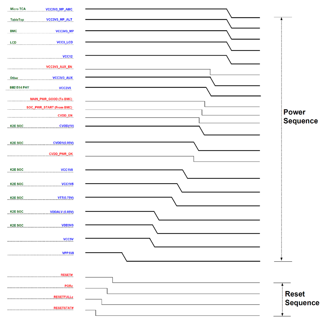
Assuming a Core before IO power up sequence table 10-2, item 2c states:
“Once CVDD is valid, the clock drivers can be enabled. Although the clock inputs are not necessary at this time, they should either be driven with a valid clock or be held in a static state with one leg high and one leg low.”
Datasheet section 10.2.1.4 also states” Note that all clock drivers should be in a high impedance state until CVDD is at a valid level and that all clock inputs be either active or in a static state with one leg pulled to ground and the other connected to CVDD.”
Figure 10-1 indicates that the clocks become active as the VDDALV rail starts to rise.
Question 1
Table 10-2, item 2c and section10.2.1.4 indicate that the clock drivers can be enabled and may be active as soon as CVDD is valid. This makes sense for the CORECLK, DDRCLK, NETCPCLK, USBCLK and SGMIICLK since these clocks use CVDD as the power domain.
However, table 9-1 indicates that the HYPLNK0CLK, PCIE0CLK, PCIE0CLK, XFICLK and TSREFCLK are associated with +1V8 power.
Is there any requirement to delay enabling of the clocks until +1V8 power is present if these clock inputs are used? (i.e. as shown visually in figure 10-1)
The concern here is that these clocks could be driving into clamp diodes of unpowered inputs.
Questions 2 & 3
Datasheet section 10.2.1 states:
“The clock input buffers for CORECLK, DDRCLK, NETCPCLK, and SGMIICLK use CVDD as a supply voltage. These clock inputs are not failsafe and must be held in a high-impedance state until CVDD is at a valid voltage level. Driving these clock inputs high before CVDD is valid could cause damage to the device. Once CVDD is valid, it is acceptable that the P and N legs of these clocks may be held in a static state (either high and low or low and high) until a valid clock frequency is needed at that input.”
Question 2
Assuming that the above inputs are AC coupled, is it acceptable to de-power the clock circuitry or to set the clock outputs close to 0V as an alternative, or can this damage the device?
Question 3
Are the any similar restrictions for the other clock inputs of the device, PCIExCLK, USBCLK, TSREFCLK etc?
Questions 4 & 5
Datasheet section 10.2.2 states:
“The power down sequence is the exact reverse of the power-up sequence described above. The goal is to prevent an excessive amount of static current and to prevent overstress of the device.”
The sequence of events detailed in table 10-2 or 10-3 indicates suggests that collapse of the CVDD1 supply should occur in the following order
DVDD33 (3V3)
VDDALV (0V85)
DVDD15 (1V5)
DVDD18 (1V8) assuming Core before IO power up
CVDD1 (or simultaneous with CVDD)
CVDD
DVDD18 (1V8) assuming IO before Core power up
The above information could be interpreted as indicating that power rails need to be equipped with sufficient bulk decoupling capacitance or hold up to allow shut down in an ordered sequence which is the reverse of that shown in Figure 10-1 or 10-2.
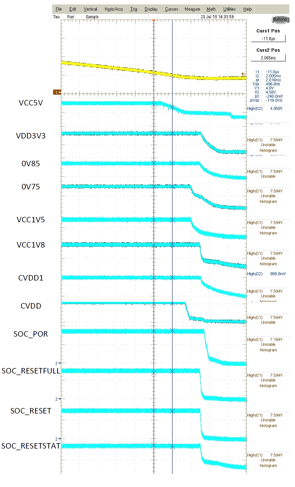
In order to try to understand this requirement we have looked at the EVMK2E evaluation board, since the processor used by this board has similar sequencing requirements shown in its datasheet.
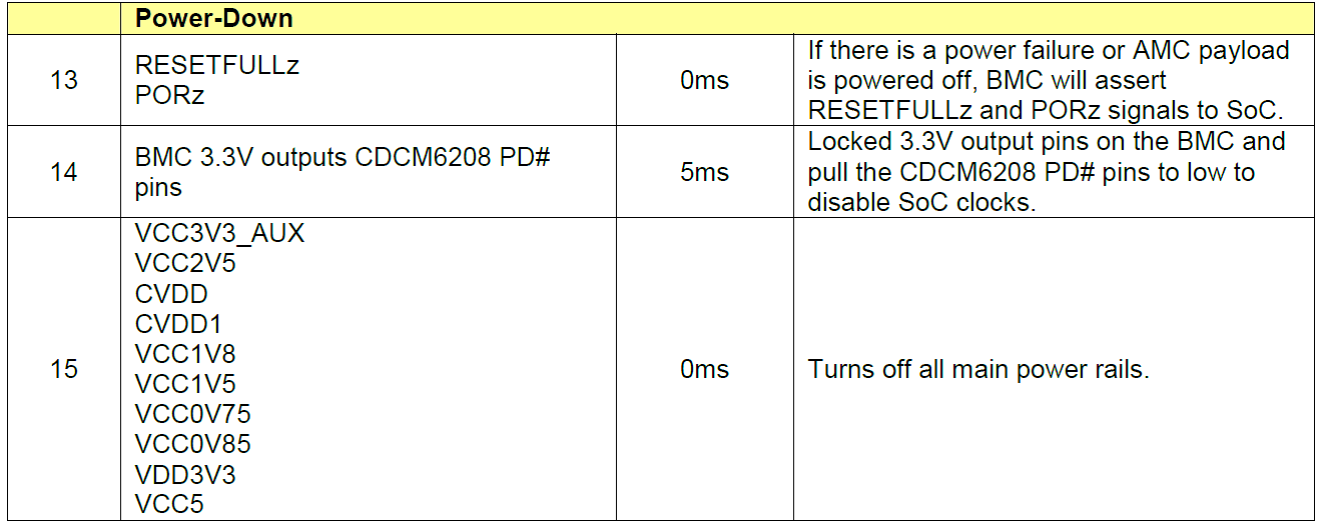
The manual for the evaluation board shows the following shutdown sequence timing settings and sequence:
Measurements performed on the EVMK2E produced the following results:
It is apparent from the shutdown sequence timing settings shown in the EVMK2E manual that no attempt is made to shut down the supplies in an orderly fashion.
The shutdown sequence measured on our EVMK2E evaluation board does not appear to meet the requirements of the processor datasheet since the variable core supply voltage collapses first CVDD. (It also does not agree with that shown in the EVMK2E manual.)
The EVMK2E solution appears to be based on fast shutdown to prevent an excessive amount of static current and to prevent overstress of the device.
Question 4
Is it acceptable during power down to turn off all AM5K2E0x supplies as quickly as possible, (as per the EVMK2E solution where the CVDD supply is turned off before all other rails have collapsed) or will this result in damage to the processor?
Question 5
Does the AM5K2E0x CVDD supply need to be provided with hold up to ensure that all other rails have collapsed before the core is depowered?
Thanks
Bob Bacon