


hi TI experts:
I meet a little issue,I hope you can help me or give me some advise。
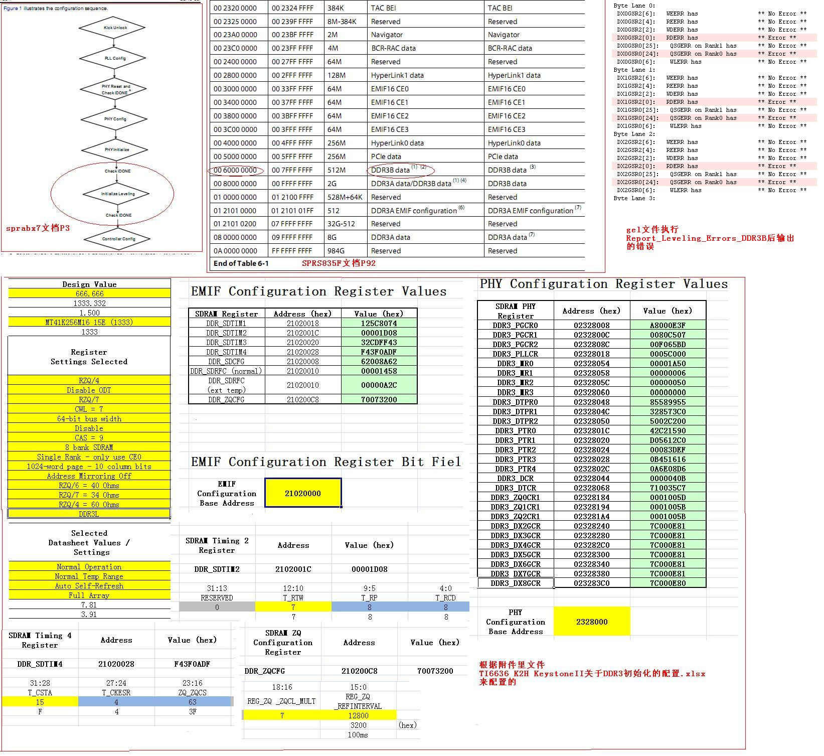
it ‘s about DDR3B in TCI6636(K2H)CPU: 66AK2Hx SR2.0, I using DDR3A interface IS43TR16512A-125KBLI and DDR3B with MT41K256M16TW-107,all 64 bit no ECC。now,address 0x80000000 can reading through DDR3A,but cann't reading DDR3B at 0x6000000,if I config DDR3B phy and EMIF by gel file,will be hang in CCS6 IDE,DDR3A is ok 。Hardware (DDR3A_REMAP_EN=1 )Accroding to TI datasheet (SPRS835F) I checked clock is 666MHz,is good。CS signal is normal and voltage is 1.5V。
Refering datasheet (sprabx7)about DDR3 Initialization sequence ,as leveling error。Attach is leveling log and DDR3B gel config files。I config DDR3B using TI6636 K2H KeystoneII adbout DDR3.xlsx ERROR is “RDERR has ERROE”。DDR3B_PGSR0 = 0xB1C001FF. DDR3A_PGSR0 = 0xB00001FF , Compare wiht log between DDR3A and DDR3B.
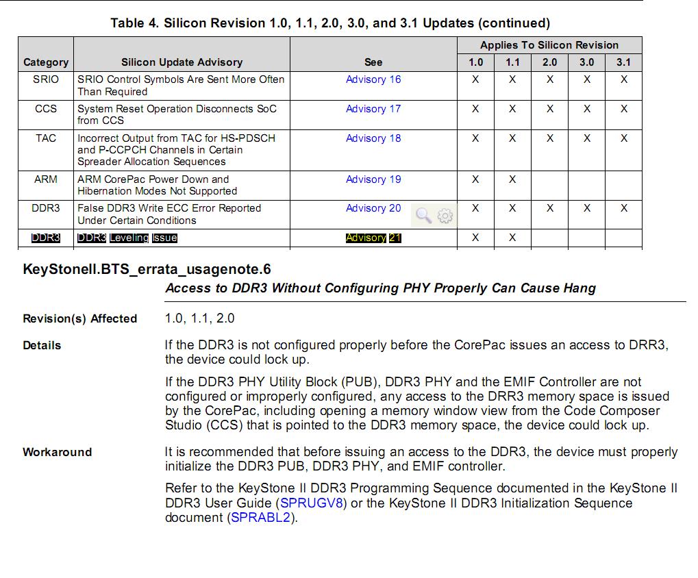
In errata,I find Advisory21 and usagenote.6 ,more likely this issue, imporperly config PUB,Phy,EMIF. So I show config as follow:
Config DDR3B function in gel File ,I promise register,or base address and offset are OK.
/*----------------------------------------------------- DDR3B : debug, 64bit--------------------------------------------------------------------------*/
ddr3B_64bit_setup(int ECC_Enable)
{ //DDR3_PLL_333
unsigned int multiplier = 19;
unsigned int divider = 0;
unsigned int OD_val = 6;
int temp,i;
int delay = 2000;
KICK0 = 0x83E70B13;
KICK1 = 0x95A4F1E0;
// Poll for IDONE=1 in the PHY General Status Register 0 (address offset 0x010).
do
{
read_val = DDR3B_PGSR0;
} while ((read_val&0x00000001) != 0x00000001);
//Clocks are enabled and frequency is stable---------------------------------------
//DDR3B PLL setup
GEL_TextOut ( "DDR3B PLL Setup ... \n");
DDR3BPLLCTL0 = DDR3BPLLCTL0 & 0xFF7FFFFF;
//Set ENSAT = 1
DDR3BPLLCTL1 |= 0x00000040;
// Put the PLL in PLL Mode
DDR3BPLLCTL0 |= 0x00800000;
//Program the necessary multipliers/dividers and BW adjustments
//Set the divider values
DDR3BPLLCTL0 &= ~(0x0000003F);
DDR3BPLLCTL0 |= (divider & 0x0000003F);
//Program OD[3:0] in the SECCTL register
DDR3BPLLCTL0 &= OUTPUT_DIVIDE_MASK; // clear the OD bit field
DDR3BPLLCTL0 |= ~OUTPUT_DIVIDE_MASK & (OD_val - 1) << OUTPUT_DIVIDE_OFFSET; // set the OD[3:0] bit field of PLLD to OD_val
// Set the Multipler values
DDR3BPLLCTL0 &= ~(0x0007FFC0);
DDR3BPLLCTL0 |= ((multiplier << 6) & 0x0007FFC0 );
// Set BWADJ
temp = ((multiplier + 1) >> 1) - 1;
DDR3BPLLCTL0 &= ~(0xFF000000);
DDR3BPLLCTL0 |= ((temp << 24) & 0xFF000000);
DDR3BPLLCTL1 &= ~(0x0000000F);
DDR3BPLLCTL1 |= ((temp >> 8) & 0x0000000F);
// In PLL Controller, reset the PLL (bit 13 in DDR3BPLLCTL1 register)
DDR3BPLLCTL1 |= 0x00004000;
for(i=0;i<delay;i++);
// In DDR3PLLCTL1, write PLLRST = 0 to bring PLL out of reset
DDR3BPLLCTL1 &= ~(0x00004000);
for(i=0;i<delay;i++);
// Put the PLL in PLL Mode Switch to PLL mode
DDR3BPLLCTL0 &= ~(0x00800000); // ReSet the Bit 23
GEL_TextOut( "Lammar DDR3 PLL Setup complete, DDR3B clock now running at 666MHz.\n" );
/*------------------------------- ECO FIX -----------------------------------------*/
/*DDR3 PHY Initialization*/
// DDR3 write leveling ECO - Assert & release DDR PHY RESET after DDR PLL setup...
DDR3BPLLCTL1 = DDR3BPLLCTL1 | 0x80000000; //Assert DDR PHY reset after PLL enabled
for(i=0;i<delay;i++); //delay 1000 cycles
DDR3BPLLCTL1 = DDR3BPLLCTL1 & 0x7FFFFFFF; //Release DDR PHY reset
do
{ // Poll IDONE after resetting PHY
read_val = DDR3B_PGSR0;
} while ((read_val&0x00000001) != 0x00000001);
/*------------------------- Start PHY Configuration -------------------------------*/
// Program FRQSEL in the PLL Control Register (address offset 0x018).
DDR3B_PLLCR = 0x0005C000; //Set FRQSEL=11, for ctl_clk between 166-275MHz
// Program WLSTEP=1, IODDRM=1, and ZCKSEL in the PHY General Configuration Register 1 (address offset 0x00C).
DDR3B_PGCR1 =0x0080C507;
// Program PHY Timing Parameters Register 0-4 (address offset 0x01C - 0x02C).
DDR3B_PTR0 = 0x42C21590;
DDR3B_PTR1 = 0xD05612C0;
DDR3B_PTR2 = 0x00083DEF;
// Maintain default values of Phy Timing Parameters Register 2 in PUB
DDR3B_PTR3 = 0x0B451616;
DDR3B_PTR4 = 0x0A6E08D6;
// Program PDQ, MPRDQ, and BYTEMASK in the DRAM Configuration Register (address offset 0x044).
// All other fields must be left at their default values.
DDR3B_DCR=0x0000040B;
read_val = DDR3B_DCR;
GEL_TextOut("DDR3B_DCR = %x\n",,,,, read_val);
//Program DRAM Timing Parameters Register 0-2 (address offset 0x048 - 0x050).
DDR3B_DTPR0 = 0x85589955;//code
DDR3B_DTPR1 = 0x328573C0;
DDR3B_DTPR2 = 0x5002C200;
// Program BL=0, CL, WR, and PD=1 in the Mode Register 0 (address offset 0x054).
// All other fields must be left at their default values.
DDR3B_MR0 = 0x00001A50;
// Program DIC, RTT, and TDQS in the Mode Register 1 (address offset 0x058).
// All other fields must be left at their default values.
DDR3B_MR1 = 0x00000006;
// Program Mode Register 2 (address offset 0x05C).
DDR3B_MR2 = 0x00000050;
DDR3B_MR3 = 0x0;
// Program DTMPR=1, DTEXD, DTEXG, RANKEN=1 or 3, and RFSHDT=7 in the Data Training Configuration Register (address offset 0x068).
// All other fields must be left at their default values.
DDR3B_DTCR = 0x710035C7; //Single-rank
// Program tREFPRD=(5*tREFI/ddr_clk_period) in the PHY General Configuration Register 2 (address offset 0x08C).
//All other fields must be left at their default values.
DDR3B_PGCR2 = 0x00F065BD;
DDR3B_PGCR0 = 0xA8000E3F;
DDR3B_PGCR1 = 0x0080C507;
//Set Impedence Register and DFIPU0=1
DDR3B_ZQ0CR1 = 0x0001005D;
DDR3B_ZQ1CR1 = 0x0001005B;
DDR3B_ZQ2CR1 = 0x0001005B;
// Re-trigger PHY initialization in DDR PHY through the VBUSP interface.
// Program 0x00000033 to the PHY Initialization Register (address offset 0x004) to re-trigger PLL, ZCAL, and DCAL initialization.
DDR3B_PIR = 0x00000033;
// Poll for IDONE=1 in the PHY General Status Register 0 (address offset 0x010).
do
{
read_val = DDR3B_PGSR0;
} while ((read_val&0x00000001) != 0x00000001);
//---------------------------------------------------------------------------------------------------------
/*DDR3B_DX2GCR = 0x7C000E81;
DDR3B_DX3GCR = 0x7C000E81;
DDR3B_DX4GCR = 0x7C000E81;
DDR3B_DX5GCR = 0x7C000E81;
DDR3B_DX6GCR = 0x7C000E81;
DDR3B_DX7GCR = 0x7C000E81;
DDR3B_DX8GCR = 0x7C000E80;*/
if(!ECC_Enable)
{
GEL_TextOut("DDR3B_DATX8_8 Front = %x\n",,,,, read_val);read_val = DDR3B_DATX8_8 ;
DDR3B_DATX8_8 = 0x7c000e80;
DDR3B_DATX8_8 = read_val & 0xFFFFFFFE; //Disable ECC byte lane
GEL_TextOut("DDR3B_DATX8_8 rear = %x\n",,,,, DDR3B_DATX8_8);
}
// Trigger DDR3 initialization and leveling/training in DDR PHY through the VBUSP interface.
// If using a 16-bit wide DDR interface, program DXEN=0 in the DATX8 2-7 General Configuration Registers (address offsets 0x240, 0x280, 0x2C0, 0x300, 0x340, and 0x380) to disable the leveling/training for the upper byte lanes.
// If using a 32-bit wide DDR interface, program DXEN=0 in the DATX8 4-7 General Configuration Registers (address offsets 0x2C0, 0x300, 0x340, and 0x380) to disable the leveling/training for the upper byte lanes.
// If ECC is not required, program DXEN=0 in the DATX8 8 General Configuration Register (address offset 0x3C0) to disable the leveling/training for the ECC byte lane.
// NOTE: Setup supports 64-bit by default, ECC enable by default.
// Program 0x0000XF81 to the PHY Initialization Register (address offset 0x004) to trigger DDR3 initialization and leveling/training sequences
DDR3B_PIR = 0x0000FF81; //WLADJ - ON
//---------------------------------------------------------------------------------------------------------
GEL_TextOut("DDR3B_leveling starting....\r\n");
// Poll for IDONE=1 in the PHY General Status Register 0 (address offset 0x010).
do {
read_val = DDR3B_PGSR0;
} while ((read_val&0x00000001) != 0x00000001);
GEL_TextOut("DDR3B_leveling over\r\n");
/* End PHY Configuration */
if(ECC_Enable)
{
GEL_TextOut("\nECC_Enable ECC_Enable ECC_Enable");
//Enable ECC
//0xB0000000: ECC_EN=1, ECC_VERIFY_EN=1, RMW_EN=1
//0x50000000: ECC_EN=1, ECC_VERIFY_EN=0, RMW_EN=1
DDR3B_ECC_CTRL = 0xB0000000;
read_val = DDR3B_ECC_CTRL;
if(read_val!=0xB0000000){
GEL_TextOut("\nIncorrect data written to DDR3B_ECC_CTRL..");
}
}
GEL_TextOut("PHY Config Complete.... \r\n");
//---------------------------------------------------------------------------------------------------------
//For single rank, EBANK field in DDR_SDCFG register needs to be programmed to 0x0.
DDR3B_SDCFG = 0x62008A62; //Single-Rank--
DDR3B_SDTIM1 = 0x125C8074;
DDR3B_SDTIM2 = 0x00001D08;
DDR3B_SDTIM3 = 0x32CDFF43;
DDR3B_SDTIM4 = 0xF43F0ADF;
//For single rank, ZQCFG needs to be programmed to 0x70073200.
DDR3B_ZQCFG = 0x70073200; //Single-Rank 0x70073200
// Program reg_initref_dis=0 in the SDRAM Refresh Control Register (address offset 0x10).
DDR3B_SDRFC = 0x00001458;//0x00000A2C
read_val = DDR3B_PGSR0;
GEL_TextOut("DDR3B_PGSR0 = %x\n",,,,, read_val);
read_val = DDR3B_PGSR1;
GEL_TextOut("DDR3B_PGSR1 = %x\n",,,,, read_val);
GEL_TextOut("DDR3B 1600 initialization complete \n");
/* End DDR3B EMIF Configuration */
}
arm_A15_0: GEL Output: DDR3B PLL Setup ...
arm_A15_0: GEL Output: Lammar DDR3 PLL Setup complete, DDR3B clock now running at 666MHz.
arm_A15_0: GEL Output: DDR3B_DCR = 0x0000040B
arm_A15_0: GEL Output: DDR3B_DATX8_8 Front = 0xB000000F
arm_A15_0: GEL Output: DDR3B_DATX8_8 rear = 0xB000000E
arm_A15_0: GEL Output: DDR3B_PGSR0 = 0xB1C001FF
arm_A15_0: GEL Output: DDR3B_PGSR1 = 0x00000000
arm_A15_0: GEL Output: DDR3B 1333 initialization complete
arm_A15_0: GEL Output: ****************************************************************************************************************
arm_A15_0: GEL Output: ********************************************************
arm_A15_0: GEL Output: ****************************************************************************************************************
arm_A15_0: GEL Output: ***************** DDR3B Leveling Errors *********************
arm_A15_0: GEL Output: PGSR0[27]: WEERR has ** No Error **
arm_A15_0: GEL Output: PGSR0[26]: REERR has ** No Error **
arm_A15_0: GEL Output: PGSR0[25]: WDERR has ** No Error **
arm_A15_0: GEL Output: PGSR0[24]: RDERR has ** Error **
arm_A15_0: GEL Output: PGSR0[23]: WLAERR has ** Error **
arm_A15_0: GEL Output: PGSR0[22]: QSGERR has ** Error **
arm_A15_0: GEL Output: PGSR0[21]: WLERR has ** No Error **
arm_A15_0: GEL Output: PGSR0[20]: ZCERR has ** No Error **
arm_A15_0: GEL Output: PGSR0[11]: WEDONE is ** Not Set **
arm_A15_0: GEL Output: PGSR0[10]: REDONE is ** Not Set **
arm_A15_0: GEL Output: PGSR0[9]: WDDONE is ** Not Set **
arm_A15_0: GEL Output: PGSR0[8]: RDDONE is ** Set **
arm_A15_0: GEL Output: PGSR0[7]: WLADONE is ** Set **
arm_A15_0: GEL Output: PGSR0[6]: QSGDONE is ** Set **
arm_A15_0: GEL Output: PGSR0[5]: WLDONE is ** Set **
arm_A15_0: GEL Output: PGSR0[4]: DIDONE is ** Set **
arm_A15_0: GEL Output: PGSR0[3]: ZCDONE is ** Not Set **
arm_A15_0: GEL Output: PGSR0[2]: DCDONE is ** Set **
arm_A15_0: GEL Output: PGSR0[1]: PLDONE is ** Set **
arm_A15_0: GEL Output: PGSR0[0]: IDONE is ** Set **
arm_A15_0: GEL Output: ********************************************************
arm_A15_0: GEL Output: Leveling Errors by Byte Lane:
arm_A15_0: GEL Output: Byte Lane 0:
arm_A15_0: GEL Output: DX0GSR2[6]: WEERR has ** No Error **
arm_A15_0: GEL Output: DX0GSR2[4]: REERR has ** No Error **
arm_A15_0: GEL Output: DX0GSR2[2]: WDERR has ** No Error **
arm_A15_0: GEL Output: DX0GSR2[0]: RDERR has ** Error **
arm_A15_0: GEL Output: DX0GSR0[25]: QSGERR on Rank1 has ** No Error **
arm_A15_0: GEL Output: DX0GSR0[24]: QSGERR on Rank0 has ** Error **
arm_A15_0: GEL Output: DX0GSR0[6]: WLERR has ** No Error **
arm_A15_0: GEL Output: Byte Lane 1:
arm_A15_0: GEL Output: DX1GSR2[6]: WEERR has ** No Error **
arm_A15_0: GEL Output: DX1GSR2[4]: REERR has ** No Error **
arm_A15_0: GEL Output: DX1GSR2[2]: WDERR has ** No Error **
arm_A15_0: GEL Output: DX1GSR2[0]: RDERR has ** Error **
arm_A15_0: GEL Output: DX1GSR0[25]: QSGERR on Rank1 has ** No Error **
arm_A15_0: GEL Output: DX1GSR0[24]: QSGERR on Rank0 has ** Error **
arm_A15_0: GEL Output: DX1GSR0[6]: WLERR has ** No Error **
arm_A15_0: GEL Output: Byte Lane 2:
arm_A15_0: GEL Output: DX2GSR2[6]: WEERR has ** No Error **
arm_A15_0: GEL Output: DX2GSR2[4]: REERR has ** No Error **
arm_A15_0: GEL Output: DX2GSR2[2]: WDERR has ** No Error **
arm_A15_0: GEL Output: DX2GSR2[0]: RDERR has ** Error **
arm_A15_0: GEL Output: DX2GSR0[25]: QSGERR on Rank1 has ** No Error **
arm_A15_0: GEL Output: DX2GSR0[24]: QSGERR on Rank0 has ** Error **
arm_A15_0: GEL Output: DX2GSR0[6]: WLERR has ** No Error **
arm_A15_0: GEL Output: Byte Lane 3:
arm_A15_0: GEL Output: DX3GSR2[6]: WEERR has ** No Error **
arm_A15_0: GEL Output: DX3GSR2[4]: REERR has ** No Error **
arm_A15_0: GEL Output: DX3GSR2[2]: WDERR has ** No Error **
arm_A15_0: GEL Output: DX3GSR2[0]: RDERR has ** Error **
arm_A15_0: GEL Output: DX3GSR0[25]: QSGERR on Rank1 has ** No Error **
arm_A15_0: GEL Output: DX3GSR0[24]: QSGERR on Rank0 has ** Error **
arm_A15_0: GEL Output: DX3GSR0[6]: WLERR has ** No Error **
arm_A15_0: GEL Output: Byte Lane 4:
arm_A15_0: GEL Output: DX4GSR2[6]: WEERR has ** No Error **
arm_A15_0: GEL Output: DX4GSR2[4]: REERR has ** No Error **
arm_A15_0: GEL Output: DX4GSR2[2]: WDERR has ** No Error **
arm_A15_0: GEL Output: DX4GSR2[0]: RDERR has ** Error **
arm_A15_0: GEL Output: DX4GSR0[25]: QSGERR on Rank1 has ** No Error **
arm_A15_0: GEL Output: DX4GSR0[24]: QSGERR on Rank0 has ** Error **
arm_A15_0: GEL Output: DX4GSR0[6]: WLERR has ** No Error **
arm_A15_0: GEL Output: Byte Lane 5:
arm_A15_0: GEL Output: DX5GSR2[6]: WEERR has ** No Error **
arm_A15_0: GEL Output: DX5GSR2[4]: REERR has ** No Error **
arm_A15_0: GEL Output: DX5GSR2[2]: WDERR has ** No Error **
arm_A15_0: GEL Output: DX5GSR2[0]: RDERR has ** Error **
arm_A15_0: GEL Output: DX5GSR0[25]: QSGERR on Rank1 has ** No Error **
arm_A15_0: GEL Output: DX5GSR0[24]: QSGERR on Rank0 has ** Error **
arm_A15_0: GEL Output: DX5GSR0[6]: WLERR has ** No Error **
arm_A15_0: GEL Output: Byte Lane 6:
arm_A15_0: GEL Output: DX6GSR2[6]: WEERR has ** No Error **
arm_A15_0: GEL Output: DX6GSR2[4]: REERR has ** No Error **
arm_A15_0: GEL Output: DX6GSR2[2]: WDERR has ** No Error **
arm_A15_0: GEL Output: DX6GSR2[0]: RDERR has ** Error **
arm_A15_0: GEL Output: DX6GSR0[25]: QSGERR on Rank1 has ** No Error **
arm_A15_0: GEL Output: DX6GSR0[24]: QSGERR on Rank0 has ** Error **
arm_A15_0: GEL Output: DX6GSR0[6]: WLERR has ** No Error **
arm_A15_0: GEL Output: Byte Lane 7:
arm_A15_0: GEL Output: DX7GSR2[6]: WEERR has ** No Error **
arm_A15_0: GEL Output: DX7GSR2[4]: REERR has ** No Error **
arm_A15_0: GEL Output: DX7GSR2[2]: WDERR has ** No Error **
arm_A15_0: GEL Output: DX7GSR2[0]: RDERR has ** Error **
arm_A15_0: GEL Output: DX7GSR0[25]: QSGERR on Rank1 has ** No Error **
arm_A15_0: GEL Output: DX7GSR0[24]: QSGERR on Rank0 has ** Error **
arm_A15_0: GEL Output: DX7GSR0[6]: WLERR has ** No Error **
arm_A15_0: GEL Output: Byte Lane 8:
arm_A15_0: GEL Output: DX8GSR2[6]: WEERR has ** No Error **
arm_A15_0: GEL Output: DX8GSR2[4]: REERR has ** No Error **
arm_A15_0: GEL Output: DX8GSR2[2]: WDERR has ** No Error **
arm_A15_0: GEL Output: DX8GSR2[0]: RDERR has ** No Error **
arm_A15_0: GEL Output: DX8GSR0[25]: QSGERR on Rank1 has ** No Error **
arm_A15_0: GEL Output: DX8GSR0[24]: QSGERR on Rank0 has ** No Error **
arm_A15_0: GEL Output: DX8GSR0[6]: WLERR has ** No Error **
arm_A15_0: GEL Output: ****************************************************************************************************************
Keystone2_DDR_Debug_v1_4_修改.gel
TI6636 K2H KeystoneII关于DDR3初始化的配置.xlsx
arm_A15_0: GEL Output: DDR3 PLL Setup ...
arm_A15_0: GEL Output: Lammar DDR3 PLL Setup complete, DDR3A clock now running at 666MHz.
arm_A15_0: GEL Output: DDR3A_DATX8_8 Front = 0xB000000F
arm_A15_0: GEL Output: DDR3A_DATX8_8 rear = 0x7C000E80
arm_A15_0: GEL Output: DDR3A_PGSR0 = 0xB0000FFF
arm_A15_0: GEL Output: DDR3A_PGSR1 = 0x00000000
arm_A15_0: GEL Output: DDR3A initialization complete

arm_A15_0: GEL Output: ****************************************************************************************************************
arm_A15_0: GEL Output: ********************************************************
arm_A15_0: GEL Output: DDR PLL Registers:

arm_A15_0: GEL Output:  DDR3A_PLL_CTL0 register:  0x092804C0 (0x02620360)
arm_A15_0: GEL Output:  	PLLD[5:0]:		0 (Pre-Divide value of 1)
arm_A15_0: GEL Output:  	PLLM[18:6]:		19 (Multiplier value of 20)
arm_A15_0: GEL Output:  	CLKOD[22:19]:		5 (Output Divide value of 6)
arm_A15_0: GEL Output:  	BYPASS[23]:		0
arm_A15_0: GEL Output:  	BWADJ-lower[31:24]: 	9
arm_A15_0: GEL Output:  DDR3A_PLL_CTL1 register:  0x00000040
arm_A15_0: GEL Output:  	PLLRESET[14]: Reset ** DEASSERTED ** to PLL
arm_A15_0: GEL Output:  	ENSAT[6]: ENSAT is SET - (GOOD)
arm_A15_0: GEL Output:  	BWADJ-upper[3:0]:	0
arm_A15_0: GEL Output:  	BWADJ[11:0] (combined):	9
arm_A15_0: GEL Output: ****************************************************************************************************************
arm_A15_0: GEL Output: ****************************************************************************************************************
arm_A15_0: GEL Output: ********************************************************
arm_A15_0: GEL Output: DDR SDRAM Configuration Register (SDCFG)
arm_A15_0: GEL Output: DDR3AEMIF_SDCFG:			0x62008C6A (Address: 0x21010008)
arm_A15_0: GEL Output: 	SDRAM Type[31:29]:   		DDR3 (3)
arm_A15_0: GEL Output: 	SDRAM Drive[27:25]:  		RZQ/4 (1)
arm_A15_0: GEL Output: 	Dynamic ODT[23:22]:  		OFF (0)
arm_A15_0: GEL Output: 	CAS Write Latency[16:14]:	7 (2)
arm_A15_0: GEL Output: 	Data Bus Width[13:12]: 		64-bit (0)
arm_A15_0: GEL Output: 	CAS Latency[11:8]:		10 (12)
arm_A15_0: GEL Output: 	Banks per SDRAM[6:5]: 		8 (3)
arm_A15_0: GEL Output: 	Chip Select Setup[3]: 		DCE0# + DCE1# (1)
arm_A15_0: GEL Output: 	Page Size[1:0]:    		1024 word page (2)
arm_A15_0: GEL Output: ********************************************************

arm_A15_0: GEL Output: ********************************************************
arm_A15_0: GEL Output: SDRAM Refresh Control Register (SDRFC)
arm_A15_0: GEL Output: DDR3AEMIF_SDRFC:			0x00000A2C (Address: 0x21010010)
arm_A15_0: GEL Output: 	INITREF_DIS[31]:		Normal operation
arm_A15_0: GEL Output: 	REFRESH_RATE[15:0]:		2604 (REFRESH_RATE = Refresh period * DDR3 clock frequency.)
arm_A15_0: GEL Output: ********************************************************

arm_A15_0: GEL Output: ********************************************************
arm_A15_0: GEL Output: SDRAM Timing 1 Register (SDTIM1)
arm_A15_0: GEL Output: DDR3AEMIF_SDTIM1:			0x125C8074 (Address: 0x21010018)
arm_A15_0: GEL Output: 	T_WR[29:25]:			9 cycles (+1)
arm_A15_0: GEL Output: 	T_RAS[24:18]:			23 cycles (+1)
arm_A15_0: GEL Output: 	T_RC[17:10]:			32 cycles (+1)
arm_A15_0: GEL Output: 	T_RRD[9:4]:			7 cycles (+1)
arm_A15_0: GEL Output: 	T_WTR[3:0]:			4 cycles (+1)
arm_A15_0: GEL Output: ********************************************************

arm_A15_0: GEL Output: ********************************************************
arm_A15_0: GEL Output: SDRAM Timing 2 Register (SDTIM2)
arm_A15_0: GEL Output: DDR3AEMIF_SDTIM2:			0x00001D08 (Address: 0x2101001C)
arm_A15_0: GEL Output: 	T_RTW[12:10]:			7 cycles (+1)
arm_A15_0: GEL Output: 	T_RP[9:5]:			8 cycles (+1)
arm_A15_0: GEL Output: 	T_RCD[4:0]:			8 cycles (+1)
arm_A15_0: GEL Output: ********************************************************

arm_A15_0: GEL Output: ********************************************************
arm_A15_0: GEL Output: SDRAM Timing 3 Register (SDTIM3)
arm_A15_0: GEL Output: DDR3AEMIF_SDTIM3:			0x32CDFF43 (Address: 0x21010020)
arm_A15_0: GEL Output: 	T_XP[31:28]:			3 cycles (+1)
arm_A15_0: GEL Output: 	T_XSNR[27:18]:			179 cycles (+1)
arm_A15_0: GEL Output: 	T_XSRD[17:8]:			511 cycles (+1)
arm_A15_0: GEL Output: 	T_RTP[7:4]:			4 cycles (+1)
arm_A15_0: GEL Output: 	T_CKE[3:0]:			3 cycles (+1)
arm_A15_0: GEL Output: ********************************************************

arm_A15_0: GEL Output: ********************************************************
arm_A15_0: GEL Output: SDRAM Timing 4 Register (SDTIM4)
arm_A15_0: GEL Output: 	DDR3AEMIF_SDTIM4:		0x543F0ADF (Address: 0x21010028)
arm_A15_0: GEL Output: 	T_CSTA[31:28]:			3 cycles (+1)
arm_A15_0: GEL Output: 	T_CKESR[27:24]:			2 cycles (+1)
arm_A15_0: GEL Output: 	ZQ_ZQCS[23:16]:			205 cycles (+1)
arm_A15_0: GEL Output: 	T_RFC[13:4]:			1012 cycles (+1)
arm_A15_0: GEL Output: 	T_RAS_MAX[3:0]:(should be 0xF)	3 cycles
arm_A15_0: GEL Output: ********************************************************

arm_A15_0: GEL Output: ********************************************************
arm_A15_0: GEL Output: SDRAM Output Impedance Calibration Configuration Register (ZQCFG)
arm_A15_0: GEL Output: 	DDR3AEMIF_ZQCFG:		0xF0073200 (Address: 0x210100C8)
arm_A15_0: GEL Output: 	ZQ_CS1EN[31]:			ZQ calibration for Rank 2 is Enabled (1)
arm_A15_0: GEL Output: 	ZQ_CS0EN[31]:			ZQ calibration for Rank 1 is Enabled (1)
arm_A15_0: GEL Output: 	ZQ_DUALCALEN[29]:		Dual ZQ calibration is Enabled (1)
arm_A15_0: GEL Output: 	ZQ_SFEXITEN[28]:		ZQ calibration on self-refresh, Active power-down and precharge power-down exit is Enabled (1)
arm_A15_0: GEL Output: 	ZQ_ZQCL_MULT[18:16]:		7 cycles
arm_A15_0: GEL Output: 	ZQ_REFINTERVAL[15:0]:		Refresh periods between ZQCS commands is 12800 (+1)
arm_A15_0: GEL Output: ********************************************************
arm_A15_0: GEL Output: ****************************************************************************************************************

arm_A15_0: GEL Output: ********************************************************
arm_A15_0: GEL Output: PLL Control Register (PLLCR)
arm_A15_0: GEL Output: DDR3A_PLLCR:			0x000DC000 (Address: 0x02329018)
arm_A15_0: GEL Output: 	FRQSEL[19:18]:			PLL Reference clock ranges from 166MHz to 275MHz (3)
arm_A15_0: GEL Output: Note: PLL Reference Clock should be 1/4 of DDR data rate. (i.e. 400MHz -> 1600MTs)
arm_A15_0: GEL Output: ********************************************************

arm_A15_0: GEL Output: ********************************************************
arm_A15_0: GEL Output: DRAM Timing Parameters Register 0 (DTPR0)
arm_A15_0: GEL Output: DDR3A_DTPR0:			0x8558AA75 (Address: 0x02329048)
arm_A15_0: GEL Output: 	tRFC[31:26]:			Activate to Activate command delay (same bank) is 33 cycles
arm_A15_0: GEL Output: 	tRRD[25:22]:			Activate to Activate command delay (diff banks) is 5 cycles
arm_A15_0: GEL Output: 	tRAS[21:16]:			Activate to Precharge command delay is 24 cycles
arm_A15_0: GEL Output: 	tRCD[15:12]:			Activate to Read/Write (on activated row) command delay is 10 cycles
arm_A15_0: GEL Output: 	tRP[11:8]:			Precharge command period is 10 cycles
arm_A15_0: GEL Output: 	tWTR[7:4]:			Internal write to read command delay is 7 cycles
arm_A15_0: GEL Output: 	tRTP[3:0]:			Internal read to precharge command delay is 5 cycles
arm_A15_0: GEL Output: ********************************************************

arm_A15_0: GEL Output: ********************************************************
arm_A15_0: GEL Output: DRAM Timing Parameters Register 1 (DTPR1)
arm_A15_0: GEL Output: DDR3A_DTPR1:			0x32857360 (Address: 0x0232904C)
arm_A15_0: GEL Output: 	tWLO[29:26]:			Write leveling output delay is 12 cycles
arm_A15_0: GEL Output: 	tWLMRD[25:20]:			Min delay from write leveling mode to first DQS edge is 40 cycles
arm_A15_0: GEL Output: 	tRFC[19:11]:			Refresh to Refresh command delay is 174 cycles
arm_A15_0: GEL Output: 	tFAW[10:5]:			4-bank activate period is 27 cycles
arm_A15_0: GEL Output: 	tMOD[4:2]:			Load mode update delay is 12 cycles (0)
arm_A15_0: GEL Output: 	tMRD[1:0]:			Load mode cycle time is 0 cycles
arm_A15_0: GEL Output: ********************************************************

arm_A15_0: GEL Output: ********************************************************
arm_A15_0: GEL Output: DRAM Timing Parameters Register 2 (DTPR2)
arm_A15_0: GEL Output: DDR3A_DTPR2:			0x5002C200 (Address: 0x02329050)
arm_A15_0: GEL Output: 	tCCD[31]:			Read to read and write to write command delay is 4 cycles (0)
arm_A15_0: GEL Output: 	tRTW[30]:			Read to write command delay is standard bus turn around delay +1 clock (1)
arm_A15_0: GEL Output: 	tRTODT[29]:			Read to ODT delay is 0, may come immediately after read post-amble (0)
arm_A15_0: GEL Output: 	tDLLK[28:19]:			DLL locking time is 512 cycles
arm_A15_0: GEL Output: 	tCKE[28:19]:			CKE minimum pulse width (tCKESR) is 5 cycles
arm_A15_0: GEL Output: 	tXP[14:10]:			Power down exit delay is 16 cycles
arm_A15_0: GEL Output: 	tXS[9:0]:			Self refresh exit delay is 512 cycles
arm_A15_0: GEL Output: ********************************************************
arm_A15_0: GEL Output: Mode Register 0 (MR0)
arm_A15_0: GEL Output: DDR3A_MR0:				0x00001A60 (Address: 0x02329054)
arm_A15_0: GEL Output: 	PD[12]:				Fast power down exit (DLL on) (1)
arm_A15_0: GEL Output: 	WR[11:9]:			Write Recovery is 10 cycles (5)
arm_A15_0: GEL Output: 	CL[6:4,2]:			10 cycles (12)
arm_A15_0: GEL Output: ********************************************************

arm_A15_0: GEL Output: ********************************************************
arm_A15_0: GEL Output: Mode Register 1 (MR1)
arm_A15_0: GEL Output: DDR3A_MR1:				0x00000006 (Address: 0x02329058)
arm_A15_0: GEL Output: 	AL[4:3]:			AL Disabled (0)
arm_A15_0: GEL Output: 	RTT[9,6,2]:			ODT is RZQ/4 on SDRAM (1)
arm_A15_0: GEL Output: 	DIC[5,1]:			Output Drive is RZQ/7 on SDRAM (1)
arm_A15_0: GEL Output: 	DE[0]:				DLL Enabled on SDRAM (0)
arm_A15_0: GEL Output: ********************************************************

arm_A15_0: GEL Output: ********************************************************
arm_A15_0: GEL Output: Mode Register 2 (MR2)
arm_A15_0: GEL Output: DDR3A_MR2:				0x00000010 (Address: 0x0232905C)
arm_A15_0: GEL Output: 	RTTWR[10:9]:			Dynamic ODT is Disabled (0)
arm_A15_0: GEL Output: 	CWL[5:3]:			CAS Write Latency is 7 cycles (2)
arm_A15_0: GEL Output: 	SRT[7]:				Normal Operating Temperature Range (0)
arm_A15_0: GEL Output: 	ASR[6]:				Auto Self-Refresh Power Management Disabled (0)
arm_A15_0: GEL Output: 	PASR[2:0]:			Partial Array Self-Refresh is set to Full Array (0)
arm_A15_0: GEL Output: ********************************************************

arm_A15_0: GEL Output: ********************************************************
arm_A15_0: GEL Output: Impedance Control Register 1 (Address/Command/Control signals) (ZQ0CR1)
arm_A15_0: GEL Output: DDR3A_ZQ0CR1:			0x0001005D (Address: 0x02329184)
arm_A15_0: GEL Output: 	ZPROG-ODT[7:4]:			On-Die Termination is set to N/A (5)
arm_A15_0: GEL Output: 	ZPROG-ZO[3:0]:			Output Impedance is set to 34ohms (13)
arm_A15_0: GEL Output: ********************************************************

arm_A15_0: GEL Output: ********************************************************
arm_A15_0: GEL Output: Impedance Control Register 1 (Data Lanes 0-3) (ZQ1CR1)
arm_A15_0: GEL Output: DDR3A_ZQ1CR1:			0x0001005B (Address: 0x02329194)
arm_A15_0: GEL Output: 	ZPROG-ODT[7:4]:			On-Die Termination is set to 60ohms (5)
arm_A15_0: GEL Output: 	ZPROG-ZO[3:0]:			Output Impedance is set to 40ohms (11)
arm_A15_0: GEL Output: ********************************************************

arm_A15_0: GEL Output: ********************************************************
arm_A15_0: GEL Output: Impedance Control Register 1 (Data Lanes 4-7) (ZQ2CR1)
arm_A15_0: GEL Output: DDR3A_ZQ2CR1:			0x0001005B (Address: 0x023291A4)
arm_A15_0: GEL Output: 	ZPROG-ODT[7:4]:			On-Die Termination is set to 60ohms (5)
arm_A15_0: GEL Output: 	ZPROG-ZO[3:0]:			Output Impedance is set to 40ohms (11)
arm_A15_0: GEL Output: ********************************************************

arm_A15_0: GEL Output: ****************************************************************************************************************
arm_A15_0: GEL Output: ***************** DDR3A Leveling Errors *********************
arm_A15_0: GEL Output:  PGSR0[27]:	WEERR has 	** No Error **
arm_A15_0: GEL Output:  PGSR0[26]:	REERR has 	** No Error **
arm_A15_0: GEL Output:  PGSR0[25]:	WDERR has 	** No Error **
arm_A15_0: GEL Output:  PGSR0[24]:	RDERR has 	** No Error **
arm_A15_0: GEL Output:  PGSR0[23]:	WLAERR has 	** No Error **
arm_A15_0: GEL Output:  PGSR0[22]:	QSGERR has 	** No Error **
arm_A15_0: GEL Output:  PGSR0[21]:	WLERR has 	** No Error **
arm_A15_0: GEL Output:  PGSR0[20]:	ZCERR has 	** No Error **

arm_A15_0: GEL Output:  PGSR0[11]:	WEDONE is 	** Set **
arm_A15_0: GEL Output:  PGSR0[10]:	REDONE is 	** Set **
arm_A15_0: GEL Output:  PGSR0[9]:		WDDONE is 	** Set **
arm_A15_0: GEL Output:  PGSR0[8]:		RDDONE is 	** Set **
arm_A15_0: GEL Output:  PGSR0[7]:		WLADONE is 	** Set **
arm_A15_0: GEL Output:  PGSR0[6]:		QSGDONE is 	** Set **
arm_A15_0: GEL Output:  PGSR0[5]:		WLDONE is 	** Set **
arm_A15_0: GEL Output:  PGSR0[4]:		DIDONE is 	** Set **
arm_A15_0: GEL Output:  PGSR0[3]:		ZCDONE is 	** Set **
arm_A15_0: GEL Output:  PGSR0[2]:		DCDONE is 	** Set **
arm_A15_0: GEL Output:  PGSR0[1]:		PLDONE is 	** Set **
arm_A15_0: GEL Output:  PGSR0[0]:		IDONE is 	** Set **

arm_A15_0: GEL Output: ********************************************************
arm_A15_0: GEL Output: Leveling Errors by Byte Lane:

arm_A15_0: GEL Output: Byte Lane 0:
arm_A15_0: GEL Output: 	DX0GSR2[6]:   WEERR has 		** No Error **
arm_A15_0: GEL Output: 	DX0GSR2[4]:   REERR has 		** No Error **
arm_A15_0: GEL Output: 	DX0GSR2[2]:   WDERR has 		** No Error **
arm_A15_0: GEL Output: 	DX0GSR2[0]:   RDERR has 		** No Error **
arm_A15_0: GEL Output: 	DX0GSR0[25]:   QSGERR on Rank1 has 	** No Error **
arm_A15_0: GEL Output: 	DX0GSR0[24]:   QSGERR on Rank0 has 	** No Error **
arm_A15_0: GEL Output: 	DX0GSR0[6]:    WLERR has 		** No Error **
arm_A15_0: GEL Output: Byte Lane 1:
arm_A15_0: GEL Output: 	DX1GSR2[6]:   WEERR has 		** No Error **
arm_A15_0: GEL Output: 	DX1GSR2[4]:   REERR has 		** No Error **
arm_A15_0: GEL Output: 	DX1GSR2[2]:   WDERR has 		** No Error **
arm_A15_0: GEL Output: 	DX1GSR2[0]:   RDERR has 		** No Error **
arm_A15_0: GEL Output: 	DX1GSR0[25]:   QSGERR on Rank1 has 	** No Error **
arm_A15_0: GEL Output: 	DX1GSR0[24]:   QSGERR on Rank0 has 	** No Error **
arm_A15_0: GEL Output: 	DX1GSR0[6]:    WLERR has 		** No Error **
arm_A15_0: GEL Output: Byte Lane 2:
arm_A15_0: GEL Output: 	DX2GSR2[6]:   WEERR has 		** No Error **
arm_A15_0: GEL Output: 	DX2GSR2[4]:   REERR has 		** No Error **
arm_A15_0: GEL Output: 	DX2GSR2[2]:   WDERR has 		** No Error **
arm_A15_0: GEL Output: 	DX2GSR2[0]:   RDERR has 		** No Error **
arm_A15_0: GEL Output: 	DX2GSR0[25]:   QSGERR on Rank1 has 	** No Error **
arm_A15_0: GEL Output: 	DX2GSR0[24]:   QSGERR on Rank0 has 	** No Error **
arm_A15_0: GEL Output: 	DX2GSR0[6]:    WLERR has 		** No Error **
arm_A15_0: GEL Output: Byte Lane 3:
arm_A15_0: GEL Output: 	DX3GSR2[6]:   WEERR has 		** No Error **
arm_A15_0: GEL Output: 	DX3GSR2[4]:   REERR has 		** No Error **
arm_A15_0: GEL Output: 	DX3GSR2[2]:   WDERR has 		** No Error **
arm_A15_0: GEL Output: 	DX3GSR2[0]:   RDERR has 		** No Error **
arm_A15_0: GEL Output: 	DX3GSR0[25]:   QSGERR on Rank1 has 	** No Error **
arm_A15_0: GEL Output: 	DX3GSR0[24]:   QSGERR on Rank0 has 	** No Error **
arm_A15_0: GEL Output: 	DX3GSR0[6]:    WLERR has 		** No Error **
arm_A15_0: GEL Output: Byte Lane 4:
arm_A15_0: GEL Output: 	DX4GSR2[6]:   WEERR has 		** No Error **
arm_A15_0: GEL Output: 	DX4GSR2[4]:   REERR has 		** No Error **
arm_A15_0: GEL Output: 	DX4GSR2[2]:   WDERR has 		** No Error **
arm_A15_0: GEL Output: 	DX4GSR2[0]:   RDERR has 		** No Error **
arm_A15_0: GEL Output: 	DX4GSR0[25]:   QSGERR on Rank1 has 	** No Error **
arm_A15_0: GEL Output: 	DX4GSR0[24]:   QSGERR on Rank0 has 	** No Error **
arm_A15_0: GEL Output: 	DX4GSR0[6]:    WLERR has 		** No Error **
arm_A15_0: GEL Output: Byte Lane 5:
arm_A15_0: GEL Output: 	DX5GSR2[6]:   WEERR has 		** No Error **
arm_A15_0: GEL Output: 	DX5GSR2[4]:   REERR has 		** No Error **
arm_A15_0: GEL Output: 	DX5GSR2[2]:   WDERR has 		** No Error **
arm_A15_0: GEL Output: 	DX5GSR2[0]:   RDERR has 		** No Error **
arm_A15_0: GEL Output: 	DX5GSR0[25]:   QSGERR on Rank1 has 	** No Error **
arm_A15_0: GEL Output: 	DX5GSR0[24]:   QSGERR on Rank0 has 	** No Error **
arm_A15_0: GEL Output: 	DX5GSR0[6]:    WLERR has 		** No Error **
arm_A15_0: GEL Output: Byte Lane 6:
arm_A15_0: GEL Output: 	DX6GSR2[6]:   WEERR has 		** No Error **
arm_A15_0: GEL Output: 	DX6GSR2[4]:   REERR has 		** No Error **
arm_A15_0: GEL Output: 	DX6GSR2[2]:   WDERR has 		** No Error **
arm_A15_0: GEL Output: 	DX6GSR2[0]:   RDERR has 		** No Error **
arm_A15_0: GEL Output: 	DX6GSR0[25]:   QSGERR on Rank1 has 	** No Error **
arm_A15_0: GEL Output: 	DX6GSR0[24]:   QSGERR on Rank0 has 	** No Error **
arm_A15_0: GEL Output: 	DX6GSR0[6]:    WLERR has 		** No Error **
arm_A15_0: GEL Output: Byte Lane 7:
arm_A15_0: GEL Output: 	DX7GSR2[6]:   WEERR has 		** No Error **
arm_A15_0: GEL Output: 	DX7GSR2[4]:   REERR has 		** No Error **
arm_A15_0: GEL Output: 	DX7GSR2[2]:   WDERR has 		** No Error **
arm_A15_0: GEL Output: 	DX7GSR2[0]:   RDERR has 		** No Error **
arm_A15_0: GEL Output: 	DX7GSR0[25]:   QSGERR on Rank1 has 	** No Error **
arm_A15_0: GEL Output: 	DX7GSR0[24]:   QSGERR on Rank0 has 	** No Error **
arm_A15_0: GEL Output: 	DX7GSR0[6]:    WLERR has 		** No Error **
arm_A15_0: GEL Output: Byte Lane 8:
arm_A15_0: GEL Output: 	DX8GSR2[6]:   WEERR has 		** No Error **
arm_A15_0: GEL Output: 	DX8GSR2[4]:   REERR has 		** No Error **
arm_A15_0: GEL Output: 	DX8GSR2[2]:   WDERR has 		** No Error **
arm_A15_0: GEL Output: 	DX8GSR2[0]:   RDERR has 		** No Error **
arm_A15_0: GEL Output: 	DX8GSR0[25]:   QSGERR on Rank1 has 	** No Error **
arm_A15_0: GEL Output: 	DX8GSR0[24]:   QSGERR on Rank0 has 	** No Error **
arm_A15_0: GEL Output: 	DX8GSR0[6]:    WLERR has 		** No Error **
arm_A15_0: GEL Output: ****************************************************************************************************************
arm_A15_0: GEL Output: ****************************************************************************************************************
arm_A15_0: GEL Output: ***************** DDR3A Leveling Values *********************
arm_A15_0: GEL Output: DDR Clock Period as measured by Leveling Registers:

arm_A15_0: GEL Output:  DX0GSR0:		0x0044A320
arm_A15_0: GEL Output:  		[14:7] (Write Leveling Period): 	6
arm_A15_0: GEL Output:  		[23:16] (Read DQS Gating Period): 	68
arm_A15_0: GEL Output:  DX1GSR0:		0x0044A2A0
arm_A15_0: GEL Output:  		[14:7] (Write Leveling Period): 	5
arm_A15_0: GEL Output:  		[23:16] (Read DQS Gating Period): 	68
arm_A15_0: GEL Output:  DX2GSR0:		0x0045A320
arm_A15_0: GEL Output:  		[14:7] (Write Leveling Period): 	6
arm_A15_0: GEL Output:  		[23:16] (Read DQS Gating Period): 	69
arm_A15_0: GEL Output:  DX3GSR0:		0x0043A2A0
arm_A15_0: GEL Output:  		[14:7] (Write Leveling Period): 	5
arm_A15_0: GEL Output:  		[23:16] (Read DQS Gating Period): 	67
arm_A15_0: GEL Output:  DX4GSR0:		0x0045A320
arm_A15_0: GEL Output:  		[14:7] (Write Leveling Period): 	6
arm_A15_0: GEL Output:  		[23:16] (Read DQS Gating Period): 	69
arm_A15_0: GEL Output:  DX5GSR0:		0x0046A320
arm_A15_0: GEL Output:  		[14:7] (Write Leveling Period): 	6
arm_A15_0: GEL Output:  		[23:16] (Read DQS Gating Period): 	70
arm_A15_0: GEL Output:  DX6GSR0:		0x0045A2A0
arm_A15_0: GEL Output:  		[14:7] (Write Leveling Period): 	5
arm_A15_0: GEL Output:  		[23:16] (Read DQS Gating Period): 	69
arm_A15_0: GEL Output:  DX7GSR0:		0x0045A2A0
arm_A15_0: GEL Output:  		[14:7] (Write Leveling Period): 	5
arm_A15_0: GEL Output:  		[23:16] (Read DQS Gating Period): 	69
arm_A15_0: GEL Output:  DX8GSR0(ECC):	0x0047A380
arm_A15_0: GEL Output:  		[14:7] (Write Leveling Period): 	7
arm_A15_0: GEL Output:  		[23:16] (Read DQS Gating Period): 	71

arm_A15_0: GEL Output: ********************************************************
arm_A15_0: GEL Output: Delay Values from Write Leveling Registers:

arm_A15_0: GEL Output:  DX0GTR:			0x00005012
arm_A15_0: GEL Output:  		[13:12] (Rank 0 WL Cycle Latency): 	1
arm_A15_0: GEL Output:  		[15:14] (Rank 1 WL Cycle Latency): 	1
arm_A15_0: GEL Output:  DX0LCDLR0:		0x00003D3D
arm_A15_0: GEL Output:  		[7:0] (Rank 0 WL Delay): 		61
arm_A15_0: GEL Output:  		[15:8] (Rank 1 WL Delay): 		61
arm_A15_0: GEL Output:  DX1GTR:			0x00005012
arm_A15_0: GEL Output:  		[13:12] (Rank 0 WL Cycle Latency): 	1
arm_A15_0: GEL Output:  		[15:14] (Rank 1 WL Cycle Latency): 	1
arm_A15_0: GEL Output:  DX1LCDLR0:		0x00003D3F
arm_A15_0: GEL Output:  		[7:0] (Rank 0 WL Delay): 		63
arm_A15_0: GEL Output:  		[15:8] (Rank 1 WL Delay): 		61
arm_A15_0: GEL Output:  DX2GTR:			0x00005012
arm_A15_0: GEL Output:  		[13:12] (Rank 0 WL Cycle Latency): 	1
arm_A15_0: GEL Output:  		[15:14] (Rank 1 WL Cycle Latency): 	1
arm_A15_0: GEL Output:  DX2LCDLR0:		0x0000393C
arm_A15_0: GEL Output:  		[7:0] (Rank 0 WL Delay): 		60
arm_A15_0: GEL Output:  		[15:8] (Rank 1 WL Delay): 		57
arm_A15_0: GEL Output:  DX3GTR:			0x00005012
arm_A15_0: GEL Output:  		[13:12] (Rank 0 WL Cycle Latency): 	1
arm_A15_0: GEL Output:  		[15:14] (Rank 1 WL Cycle Latency): 	1
arm_A15_0: GEL Output:  DX3LCDLR0:		0x0000383C
arm_A15_0: GEL Output:  		[7:0] (Rank 0 WL Delay): 		60
arm_A15_0: GEL Output:  		[15:8] (Rank 1 WL Delay): 		56
arm_A15_0: GEL Output:  DX4GTR:			0x00005012
arm_A15_0: GEL Output:  		[13:12] (Rank 0 WL Cycle Latency): 	1
arm_A15_0: GEL Output:  		[15:14] (Rank 1 WL Cycle Latency): 	1
arm_A15_0: GEL Output:  DX4LCDLR0:		0x00000807
arm_A15_0: GEL Output:  		[7:0] (Rank 0 WL Delay): 		7
arm_A15_0: GEL Output:  		[15:8] (Rank 1 WL Delay): 		8
arm_A15_0: GEL Output:  DX5GTR:			0x00005012
arm_A15_0: GEL Output:  		[13:12] (Rank 0 WL Cycle Latency): 	1
arm_A15_0: GEL Output:  		[15:14] (Rank 1 WL Cycle Latency): 	1
arm_A15_0: GEL Output:  DX5LCDLR0:		0x00001010
arm_A15_0: GEL Output:  		[7:0] (Rank 0 WL Delay): 		16
arm_A15_0: GEL Output:  		[15:8] (Rank 1 WL Delay): 		16
arm_A15_0: GEL Output:  DX6GTR:			0x00005012
arm_A15_0: GEL Output:  		[13:12] (Rank 0 WL Cycle Latency): 	1
arm_A15_0: GEL Output:  		[15:14] (Rank 1 WL Cycle Latency): 	1
arm_A15_0: GEL Output:  DX6LCDLR0:		0x00000F13
arm_A15_0: GEL Output:  		[7:0] (Rank 0 WL Delay): 		19
arm_A15_0: GEL Output:  		[15:8] (Rank 1 WL Delay): 		15
arm_A15_0: GEL Output:  DX7GTR:			0x00005012
arm_A15_0: GEL Output:  		[13:12] (Rank 0 WL Cycle Latency): 	1
arm_A15_0: GEL Output:  		[15:14] (Rank 1 WL Cycle Latency): 	1
arm_A15_0: GEL Output:  DX7LCDLR0:		0x00001015
arm_A15_0: GEL Output:  		[7:0] (Rank 0 WL Delay): 		21
arm_A15_0: GEL Output:  		[15:8] (Rank 1 WL Delay): 		16
arm_A15_0: GEL Output:  DX8GTR:			0x00005000
arm_A15_0: GEL Output:  		[13:12] (Rank 0 WL Cycle Latency): 	1
arm_A15_0: GEL Output:  		[15:14] (Rank 1 WL Cycle Latency): 	1
arm_A15_0: GEL Output:  DX8LCDLR0:		0x00000000
arm_A15_0: GEL Output:  		[7:0] (Rank 0 WL Delay): 		0
arm_A15_0: GEL Output:  		[15:8] (Rank 1 WL Delay): 		0
arm_A15_0: GEL Output: ********************************************************
arm_A15_0: GEL Output: Equivalent 90 degree phase shift in delay units, derived from measured period:

arm_A15_0: GEL Output:  DX0LCDLR1:		0x00211F27
arm_A15_0: GEL Output:  		[7:0] (Write Delay Shift): 		39
arm_A15_0: GEL Output:  		[15:8] (Read DQS Delay):		31
arm_A15_0: GEL Output:  		[23:16] (Read DQSN Delay): 		33
arm_A15_0: GEL Output:  DX1LCDLR1:		0x001E1E29
arm_A15_0: GEL Output:  		[7:0] (Write Delay Shift): 		41
arm_A15_0: GEL Output:  		[15:8] (Read DQS Delay): 		30
arm_A15_0: GEL Output:  		[23:16] (Read DQSN Delay): 		30
arm_A15_0: GEL Output:  DX2LCDLR1:		0x00202029
arm_A15_0: GEL Output:  		[7:0] (Write Delay Shift): 		41
arm_A15_0: GEL Output:  		[15:8] (Read DQS Delay): 		32
arm_A15_0: GEL Output:  		[23:16] (Read DQSN Delay): 		32
arm_A15_0: GEL Output:  DX3LCDLR1:		0x001D1D28
arm_A15_0: GEL Output:  		[7:0] (Write Delay Shift): 		40
arm_A15_0: GEL Output:  		[15:8] (Read DQS Delay): 		29
arm_A15_0: GEL Output:  		[23:16] (Read DQSN Delay): 		29
arm_A15_0: GEL Output:  DX4LCDLR1:		0x001E1E29
arm_A15_0: GEL Output:  		[7:0] (Write Delay Shift): 		41
arm_A15_0: GEL Output:  		[15:8] (Read DQS Delay): 		30
arm_A15_0: GEL Output:  		[23:16] (Read DQSN Delay): 		30
arm_A15_0: GEL Output:  DX5LCDLR1:		0x001E1E28
arm_A15_0: GEL Output:  		[7:0] (Write Delay Shift): 		40
arm_A15_0: GEL Output:  		[15:8] (Read DQS Delay): 		30
arm_A15_0: GEL Output:  		[23:16] (Read DQSN Delay): 		30
arm_A15_0: GEL Output:  DX6LCDLR1:		0x00202027
arm_A15_0: GEL Output:  		[7:0] (Write Delay Shift): 		39
arm_A15_0: GEL Output:  		[15:8] (Read DQS Delay): 		32
arm_A15_0: GEL Output:  		[23:16] (Read DQSN Delay): 		32
arm_A15_0: GEL Output:  DX7LCDLR1:		0x001F1F27
arm_A15_0: GEL Output:  		[7:0] (Write Delay Shift): 		39
arm_A15_0: GEL Output:  		[15:8] (Read DQS Delay): 		31
arm_A15_0: GEL Output:  		[23:16] (Read DQSN Delay): 		31
arm_A15_0: GEL Output:  DX8LCDLR1:		0x00232322
arm_A15_0: GEL Output:  		[7:0] (Write Delay Shift): 		34
arm_A15_0: GEL Output:  		[15:8] (Read DQS Delay): 		35
arm_A15_0: GEL Output:  		[23:16] (Read DQSN Delay): 		35
arm_A15_0: GEL Output: ********************************************************
arm_A15_0: GEL Output: Delay Values from Read DQS Gating Leveling Registers:

arm_A15_0: GEL Output:  DX0GTR:			0x00005012
arm_A15_0: GEL Output:  		[2:0] (Rank 0 DQS Gating Latency): 	2
arm_A15_0: GEL Output:  		[5:3] (Rank 1 DQS Gating Latency): 	2
arm_A15_0: GEL Output:  DX0LCDLR2:		0x00004D4D
arm_A15_0: GEL Output:  		[7:0] (Rank 0 RL Delay): 		77
arm_A15_0: GEL Output:  		[15:8] (Rank 1 RL Delay): 		77
arm_A15_0: GEL Output:  DX1GTR:			0x00005012
arm_A15_0: GEL Output:  		[2:0] (Rank 0 DQS Gating Latency): 	2
arm_A15_0: GEL Output:  		[5:3] (Rank 1 DQS Gating Latency): 	2
arm_A15_0: GEL Output:  DX1LCDLR2:		0x0000494A
arm_A15_0: GEL Output:  		[7:0] (Rank 0 RL Delay): 		74
arm_A15_0: GEL Output:  		[15:8] (Rank 1 RL Delay): 		73
arm_A15_0: GEL Output:  DX2GTR:			0x00005012
arm_A15_0: GEL Output:  		[2:0] (Rank 0 DQS Gating Latency): 	2
arm_A15_0: GEL Output:  		[5:3] (Rank 1 DQS Gating Latency): 	2
arm_A15_0: GEL Output:  DX2LCDLR2:		0x00005051
arm_A15_0: GEL Output:  		[7:0] (Rank 0 RL Delay): 		81
arm_A15_0: GEL Output:  		[15:8] (Rank 1 RL Delay): 		80
arm_A15_0: GEL Output:  DX3GTR:			0x00005012
arm_A15_0: GEL Output:  		[2:0] (Rank 0 DQS Gating Latency): 	2
arm_A15_0: GEL Output:  		[5:3] (Rank 1 DQS Gating Latency): 	2
arm_A15_0: GEL Output:  DX3LCDLR2:		0x00004949
arm_A15_0: GEL Output:  		[7:0] (Rank 0 RL Delay): 		73
arm_A15_0: GEL Output:  		[15:8] (Rank 1 RL Delay): 		73
arm_A15_0: GEL Output:  DX4GTR:			0x00005012
arm_A15_0: GEL Output:  		[2:0] (Rank 0 DQS Gating Latency): 	2
arm_A15_0: GEL Output:  		[5:3] (Rank 1 DQS Gating Latency): 	2
arm_A15_0: GEL Output:  DX4LCDLR2:		0x00002526
arm_A15_0: GEL Output:  		[7:0] (Rank 0 RL Delay): 		38
arm_A15_0: GEL Output:  		[15:8] (Rank 1 RL Delay): 		37
arm_A15_0: GEL Output:  DX5GTR:			0x00005012
arm_A15_0: GEL Output:  		[2:0] (Rank 0 DQS Gating Latency): 	2
arm_A15_0: GEL Output:  		[5:3] (Rank 1 DQS Gating Latency): 	2
arm_A15_0: GEL Output:  DX5LCDLR2:		0x00001719
arm_A15_0: GEL Output:  		[7:0] (Rank 0 RL Delay): 		25
arm_A15_0: GEL Output:  		[15:8] (Rank 1 RL Delay): 		23
arm_A15_0: GEL Output:  DX6GTR:			0x00005012
arm_A15_0: GEL Output:  		[2:0] (Rank 0 DQS Gating Latency): 	2
arm_A15_0: GEL Output:  		[5:3] (Rank 1 DQS Gating Latency): 	2
arm_A15_0: GEL Output:  DX6LCDLR2:		0x00001C21
arm_A15_0: GEL Output:  		[7:0] (Rank 0 RL Delay): 		33
arm_A15_0: GEL Output:  		[15:8] (Rank 1 RL Delay): 		28
arm_A15_0: GEL Output:  DX7GTR:			0x00005012
arm_A15_0: GEL Output:  		[2:0] (Rank 0 DQS Gating Latency): 	2
arm_A15_0: GEL Output:  		[5:3] (Rank 1 DQS Gating Latency): 	2
arm_A15_0: GEL Output:  DX7LCDLR2:		0x00001A1F
arm_A15_0: GEL Output:  		[7:0] (Rank 0 RL Delay): 		31
arm_A15_0: GEL Output:  		[15:8] (Rank 1 RL Delay): 		26
arm_A15_0: GEL Output:  DX8GTR:			0x00005000
arm_A15_0: GEL Output:  		[2:0] (Rank 0 DQS Gating Latency): 	0
arm_A15_0: GEL Output:  		[5:3] (Rank 1 DQS Gating Latency): 	0
arm_A15_0: GEL Output:  DX8LCDLR2:		0x00000000
arm_A15_0: GEL Output:  		[7:0] (Rank 0 RL Delay): 		0
arm_A15_0: GEL Output:  		[15:8] (Rank 1 RL Delay): 		0
arm_A15_0: GEL Output: ****************************************************************************************************************
arm_A15_0: GEL Output: DDR3B PLL Setup ...
arm_A15_0: GEL Output: Lammar DDR3 PLL Setup complete, DDR3B clock now running at 666MHz.
arm_A15_0: GEL Output: DDR3B_DCR = 0x0000040B
arm_A15_0: GEL Output: DDR3B_DATX8_8 Front = 0xB000000F
arm_A15_0: GEL Output: DDR3B_DATX8_8 rear = 0xB000000E
arm_A15_0: GEL Output: DDR3B_PGSR0 = 0xB1C001FF
arm_A15_0: GEL Output: DDR3B_PGSR1 = 0x00000000
arm_A15_0: GEL Output: DDR3B 1600 initialization complete
arm_A15_0: GEL Output: ****************************************************************************************************************
arm_A15_0: GEL Output: ********************************************************
arm_A15_0: GEL Output: DDR PLL Registers:

arm_A15_0: GEL Output:  DDR3B_PLL_CTL0 register:  0x092804C0 (0x02620368)
arm_A15_0: GEL Output:  	PLLD[5:0]:		0 (Pre-Divide value of 1)
arm_A15_0: GEL Output:  	PLLM[18:6]:		19 (Multiplier value of 20)
arm_A15_0: GEL Output:  	CLKOD[22:19]:		5 (Output Divide value of 6)
arm_A15_0: GEL Output:  	BYPASS[23]:		0
arm_A15_0: GEL Output:  	BWADJ-lower[31:24]: 	9
arm_A15_0: GEL Output:  DDR3B_PLL_CTL1 register:  0x00000040
arm_A15_0: GEL Output:  	PLLRESET[14]: Reset ** DEASSERTED ** to PLL
arm_A15_0: GEL Output:  	ENSAT[6]: ENSAT is SET - (GOOD)
arm_A15_0: GEL Output:  	BWADJ-upper[3:0]:	0
arm_A15_0: GEL Output:  	BWADJ[11:0] (combined):	9
arm_A15_0: GEL Output: ****************************************************************************************************************
arm_A15_0: GEL Output: ****************************************************************************************************************
arm_A15_0: GEL Output: ********************************************************
arm_A15_0: GEL Output: DDR SDRAM Configuration Register (SDCFG)
arm_A15_0: GEL Output: DDR3BEMIF_SDCFG:			0x6200CE62 (Address: 0x21020008)
arm_A15_0: GEL Output: 	SDRAM Type[31:29]:   		DDR3 (3)
arm_A15_0: GEL Output: 	SDRAM Drive[27:25]:  		RZQ/4 (1)
arm_A15_0: GEL Output: 	Dynamic ODT[23:22]:  		OFF (0)
arm_A15_0: GEL Output: 	CAS Write Latency[16:14]:	8 (3)
arm_A15_0: GEL Output: 	Data Bus Width[13:12]: 		64-bit (0)
arm_A15_0: GEL Output: 	CAS Latency[11:8]:		11 (14)
arm_A15_0: GEL Output: 	Banks per SDRAM[6:5]: 		8 (3)
arm_A15_0: GEL Output: 	Chip Select Setup[3]: 		DCE0# (0)
arm_A15_0: GEL Output: 	Page Size[1:0]:    		1024 word page (2)
arm_A15_0: GEL Output: ********************************************************

arm_A15_0: GEL Output: ********************************************************
arm_A15_0: GEL Output: SDRAM Refresh Control Register (SDRFC)
arm_A15_0: GEL Output: DDR3BEMIF_SDRFC:			0x00001869 (Address: 0x21020010)
arm_A15_0: GEL Output: 	INITREF_DIS[31]:		Normal operation
arm_A15_0: GEL Output: 	REFRESH_RATE[15:0]:		6249 (REFRESH_RATE = Refresh period * DDR3 clock frequency.)
arm_A15_0: GEL Output: ********************************************************

arm_A15_0: GEL Output: ********************************************************
arm_A15_0: GEL Output: SDRAM Timing 1 Register (SDTIM1)
arm_A15_0: GEL Output: DDR3BEMIF_SDTIM1:			0x166C9855 (Address: 0x21020018)
arm_A15_0: GEL Output: 	T_WR[29:25]:			11 cycles (+1)
arm_A15_0: GEL Output: 	T_RAS[24:18]:			27 cycles (+1)
arm_A15_0: GEL Output: 	T_RC[17:10]:			38 cycles (+1)
arm_A15_0: GEL Output: 	T_RRD[9:4]:			5 cycles (+1)
arm_A15_0: GEL Output: 	T_WTR[3:0]:			5 cycles (+1)
arm_A15_0: GEL Output: ********************************************************

arm_A15_0: GEL Output: ********************************************************
arm_A15_0: GEL Output: SDRAM Timing 2 Register (SDTIM2)
arm_A15_0: GEL Output: DDR3BEMIF_SDTIM2:			0x00001D4A (Address: 0x2102001C)
arm_A15_0: GEL Output: 	T_RTW[12:10]:			7 cycles (+1)
arm_A15_0: GEL Output: 	T_RP[9:5]:			10 cycles (+1)
arm_A15_0: GEL Output: 	T_RCD[4:0]:			10 cycles (+1)
arm_A15_0: GEL Output: ********************************************************

arm_A15_0: GEL Output: ********************************************************
arm_A15_0: GEL Output: SDRAM Timing 3 Register (SDTIM3)
arm_A15_0: GEL Output: DDR3BEMIF_SDTIM3:			0x35DFF53A (Address: 0x21020020)
arm_A15_0: GEL Output: 	T_XP[31:28]:			3 cycles (+1)
arm_A15_0: GEL Output: 	T_XSNR[27:18]:			375 cycles (+1)
arm_A15_0: GEL Output: 	T_XSRD[17:8]:			1013 cycles (+1)
arm_A15_0: GEL Output: 	T_RTP[7:4]:			3 cycles (+1)
arm_A15_0: GEL Output: 	T_CKE[3:0]:			10 cycles (+1)
arm_A15_0: GEL Output: ********************************************************

arm_A15_0: GEL Output: ********************************************************
arm_A15_0: GEL Output: SDRAM Timing 4 Register (SDTIM4)
arm_A15_0: GEL Output: 	DDR3BEMIF_SDTIM4:		0x543F0CFF (Address: 0x21020028)
arm_A15_0: GEL Output: 	T_CSTA[31:28]:			3 cycles (+1)
arm_A15_0: GEL Output: 	T_CKESR[27:24]:			5 cycles (+1)
arm_A15_0: GEL Output: 	ZQ_ZQCS[23:16]:			223 cycles (+1)
arm_A15_0: GEL Output: 	T_RFC[13:4]:			851 cycles (+1)
arm_A15_0: GEL Output: 	T_RAS_MAX[3:0]:(should be 0xF)	10 cycles
arm_A15_0: GEL Output: ********************************************************

arm_A15_0: GEL Output: ********************************************************
arm_A15_0: GEL Output: SDRAM Output Impedance Calibration Configuration Register (ZQCFG)
arm_A15_0: GEL Output: 	DDR3BEMIF_ZQCFG:		0x70073200 (Address: 0x210200C8)
arm_A15_0: GEL Output: 	ZQ_CS1EN[31]:			ZQ calibration for Rank 2 is Disabled (0)
arm_A15_0: GEL Output: 	ZQ_CS0EN[31]:			ZQ calibration for Rank 1 is Enabled (1)
arm_A15_0: GEL Output: 	ZQ_DUALCALEN[29]:		Dual ZQ calibration is Enabled (1)
arm_A15_0: GEL Output: 	ZQ_SFEXITEN[28]:		ZQ calibration on self-refresh, Active power-down and precharge power-down exit is Enabled (1)
arm_A15_0: GEL Output: 	ZQ_ZQCL_MULT[18:16]:		7 cycles
arm_A15_0: GEL Output: 	ZQ_REFINTERVAL[15:0]:		Refresh periods between ZQCS commands is 12800 (+1)
arm_A15_0: GEL Output: ********************************************************
arm_A15_0: GEL Output: ****************************************************************************************************************

arm_A15_0: GEL Output: ********************************************************
arm_A15_0: GEL Output: PLL Control Register (PLLCR)
arm_A15_0: GEL Output: DDR3B_PLLCR:			0x000DE000 (Address: 0x02328018)
arm_A15_0: GEL Output: 	FRQSEL[19:18]:			PLL Reference clock ranges from 166MHz to 275MHz (3)
arm_A15_0: GEL Output: Note: PLL Reference Clock should be 1/4 of DDR data rate. (i.e. 400MHz -> 1600MTs)
arm_A15_0: GEL Output: ********************************************************

arm_A15_0: GEL Output: ********************************************************
arm_A15_0: GEL Output: DRAM Timing Parameters Register 0 (DTPR0)
arm_A15_0: GEL Output: DDR3B_DTPR0:			0x8558AA75 (Address: 0x02328048)
arm_A15_0: GEL Output: 	tRFC[31:26]:			Activate to Activate command delay (same bank) is 33 cycles
arm_A15_0: GEL Output: 	tRRD[25:22]:			Activate to Activate command delay (diff banks) is 5 cycles
arm_A15_0: GEL Output: 	tRAS[21:16]:			Activate to Precharge command delay is 24 cycles
arm_A15_0: GEL Output: 	tRCD[15:12]:			Activate to Read/Write (on activated row) command delay is 10 cycles
arm_A15_0: GEL Output: 	tRP[11:8]:			Precharge command period is 10 cycles
arm_A15_0: GEL Output: 	tWTR[7:4]:			Internal write to read command delay is 7 cycles
arm_A15_0: GEL Output: 	tRTP[3:0]:			Internal read to precharge command delay is 5 cycles
arm_A15_0: GEL Output: ********************************************************

arm_A15_0: GEL Output: ********************************************************
arm_A15_0: GEL Output: DRAM Timing Parameters Register 1 (DTPR1)
arm_A15_0: GEL Output: DDR3B_DTPR1:			0x32857370 (Address: 0x0232804C)
arm_A15_0: GEL Output: 	tWLO[29:26]:			Write leveling output delay is 12 cycles
arm_A15_0: GEL Output: 	tWLMRD[25:20]:			Min delay from write leveling mode to first DQS edge is 40 cycles
arm_A15_0: GEL Output: 	tRFC[19:11]:			Refresh to Refresh command delay is 174 cycles
arm_A15_0: GEL Output: 	tFAW[10:5]:			4-bank activate period is 27 cycles
arm_A15_0: GEL Output: 	tMOD[4:2]:			Load mode update delay is Reserved Value cycles (16)
arm_A15_0: GEL Output: 	tMRD[1:0]:			Load mode cycle time is 0 cycles
arm_A15_0: GEL Output: ********************************************************

arm_A15_0: GEL Output: ********************************************************
arm_A15_0: GEL Output: DRAM Timing Parameters Register 2 (DTPR2)
arm_A15_0: GEL Output: DDR3B_DTPR2:			0x5002C200 (Address: 0x02328050)
arm_A15_0: GEL Output: 	tCCD[31]:			Read to read and write to write command delay is 4 cycles (0)
arm_A15_0: GEL Output: 	tRTW[30]:			Read to write command delay is standard bus turn around delay +1 clock (1)
arm_A15_0: GEL Output: 	tRTODT[29]:			Read to ODT delay is 0, may come immediately after read post-amble (0)
arm_A15_0: GEL Output: 	tDLLK[28:19]:			DLL locking time is 512 cycles
arm_A15_0: GEL Output: 	tCKE[28:19]:			CKE minimum pulse width (tCKESR) is 5 cycles
arm_A15_0: GEL Output: 	tXP[14:10]:			Power down exit delay is 16 cycles
arm_A15_0: GEL Output: 	tXS[9:0]:			Self refresh exit delay is 512 cycles
arm_A15_0: GEL Output: ********************************************************
arm_A15_0: GEL Output: Mode Register 0 (MR0)
arm_A15_0: GEL Output: DDR3B_MR0:				0x00001C70 (Address: 0x02328054)
arm_A15_0: GEL Output: 	PD[12]:				Fast power down exit (DLL on) (1)
arm_A15_0: GEL Output: 	WR[11:9]:Write Recovery is 14 cycles (6)
arm_A15_0: GEL Output: 	CL[6:4,2]:			11 cycles (14)
arm_A15_0: GEL Output: ********************************************************

arm_A15_0: GEL Output: ********************************************************
arm_A15_0: GEL Output: Mode Register 1 (MR1)
arm_A15_0: GEL Output: DDR3B_MR1:				0x00000006 (Address: 0x02328058)
arm_A15_0: GEL Output: 	AL[4:3]:			AL Disabled (0)
arm_A15_0: GEL Output: 	RTT[9,6,2]:			ODT is RZQ/4 on SDRAM (1)
arm_A15_0: GEL Output: 	DIC[5,1]:			Output Drive is RZQ/7 on SDRAM (1)
arm_A15_0: GEL Output: 	DE[0]:				DLL Enabled on SDRAM (0)
arm_A15_0: GEL Output: ********************************************************

arm_A15_0: GEL Output: ********************************************************
arm_A15_0: GEL Output: Mode Register 2 (MR2)
arm_A15_0: GEL Output: DDR3B_MR2:				0x00000018 (Address: 0x0232805C)
arm_A15_0: GEL Output: 	RTTWR[10:9]:			Dynamic ODT is Disabled (0)
arm_A15_0: GEL Output: 	CWL[5:3]:			CAS Write Latency is 8 cycles (3)
arm_A15_0: GEL Output: 	SRT[7]:				Normal Operating Temperature Range (0)
arm_A15_0: GEL Output: 	ASR[6]:				Auto Self-Refresh Power Management Disabled (0)
arm_A15_0: GEL Output: 	PASR[2:0]:			Partial Array Self-Refresh is set to Full Array (0)
arm_A15_0: GEL Output: ********************************************************

arm_A15_0: GEL Output: ********************************************************
arm_A15_0: GEL Output: Impedance Control Register 1 (ACC signals) (ZQ0CR1)
arm_A15_0: GEL Output: DDR3B_ZQ0CR1:			0x0001005D (Address: 0x02328184)
arm_A15_0: GEL Output: 	ZPROG-ODT[7:4]:			On-Die Termination is set to N/A (5)
arm_A15_0: GEL Output: 	ZPROG-ZO[3:0]:			Output Impedance is set to 34ohms (13)
arm_A15_0: GEL Output: ********************************************************

arm_A15_0: GEL Output: ********************************************************
arm_A15_0: GEL Output: Impedance Control Register 1 (Data Lanes 0-3) (ZQ1CR1)
arm_A15_0: GEL Output: DDR3B_ZQ1CR1:			0x0001005B (Address: 0x02328194)
arm_A15_0: GEL Output: 	ZPROG-ODT[7:4]:			On-Die Termination is set to 60ohms (5)
arm_A15_0: GEL Output: 	ZPROG-ZO[3:0]:			Output Impedance is set to 40ohms (11)
arm_A15_0: GEL Output: ********************************************************

arm_A15_0: GEL Output: ********************************************************
arm_A15_0: GEL Output: Impedance Control Register 1 (Data Lanes 4-7) (ZQ2CR1)
arm_A15_0: GEL Output: DDR3B_ZQ2CR1:			0x0001005B (Address: 0x023281A4)
arm_A15_0: GEL Output: 	ZPROG-ODT[7:4]:			On-Die Termination is set to 60ohms (5)
arm_A15_0: GEL Output: 	ZPROG-ZO[3:0]:			Output Impedance is set to 40ohms (11)
arm_A15_0: GEL Output: ********************************************************

arm_A15_0: GEL Output: ****************************************************************************************************************
arm_A15_0: GEL Output: ***************** DDR3B Leveling Errors *********************
arm_A15_0: GEL Output:  PGSR0[27]:	WEERR has 	** No Error **
arm_A15_0: GEL Output:  PGSR0[26]:	REERR has 	** No Error **
arm_A15_0: GEL Output:  PGSR0[25]:	WDERR has 	** No Error **
arm_A15_0: GEL Output:  PGSR0[24]:	RDERR has 	** Error **
arm_A15_0: GEL Output:  PGSR0[23]:	WLAERR has 	** Error **
arm_A15_0: GEL Output:  PGSR0[22]:	QSGERR has 	** Error **
arm_A15_0: GEL Output:  PGSR0[21]:	WLERR has 	** No Error **
arm_A15_0: GEL Output:  PGSR0[20]:	ZCERR has 	** No Error **

arm_A15_0: GEL Output:  PGSR0[11]:	WEDONE is 	** Not Set **
arm_A15_0: GEL Output:  PGSR0[10]:	REDONE is 	** Not Set **
arm_A15_0: GEL Output:  PGSR0[9]:		WDDONE is 	** Not Set **
arm_A15_0: GEL Output:  PGSR0[8]:		RDDONE is 	** Set **
arm_A15_0: GEL Output:  PGSR0[7]:		WLADONE is 	** Set **
arm_A15_0: GEL Output:  PGSR0[6]:		QSGDONE is 	** Set **
arm_A15_0: GEL Output:  PGSR0[5]:		WLDONE is 	** Set **
arm_A15_0: GEL Output:  PGSR0[4]:		DIDONE is 	** Set **
arm_A15_0: GEL Output:  PGSR0[3]:		ZCDONE is 	** Not Set **
arm_A15_0: GEL Output:  PGSR0[2]:		DCDONE is 	** Set **
arm_A15_0: GEL Output:  PGSR0[1]:		PLDONE is 	** Set **
arm_A15_0: GEL Output:  PGSR0[0]:		IDONE is 	** Set **

arm_A15_0: GEL Output: ********************************************************
arm_A15_0: GEL Output: Leveling Errors by Byte Lane:

arm_A15_0: GEL Output: Byte Lane 0:
arm_A15_0: GEL Output: 	DX0GSR2[6]:   WEERR has 		** No Error **
arm_A15_0: GEL Output: 	DX0GSR2[4]:   REERR has 		** No Error **
arm_A15_0: GEL Output: 	DX0GSR2[2]:   WDERR has 		** No Error **
arm_A15_0: GEL Output: 	DX0GSR2[0]:   RDERR has 		** Error **
arm_A15_0: GEL Output: 	DX0GSR0[25]:   QSGERR on Rank1 has 	** No Error **
arm_A15_0: GEL Output: 	DX0GSR0[24]:   QSGERR on Rank0 has 	** Error **
arm_A15_0: GEL Output: 	DX0GSR0[6]:    WLERR has 		** No Error **
arm_A15_0: GEL Output: Byte Lane 1:
arm_A15_0: GEL Output: 	DX1GSR2[6]:   WEERR has 		** No Error **
arm_A15_0: GEL Output: 	DX1GSR2[4]:   REERR has 		** No Error **
arm_A15_0: GEL Output: 	DX1GSR2[2]:   WDERR has 		** No Error **
arm_A15_0: GEL Output: 	DX1GSR2[0]:   RDERR has 		** Error **
arm_A15_0: GEL Output: 	DX1GSR0[25]:   QSGERR on Rank1 has 	** No Error **
arm_A15_0: GEL Output: 	DX1GSR0[24]:   QSGERR on Rank0 has 	** Error **
arm_A15_0: GEL Output: 	DX1GSR0[6]:    WLERR has 		** No Error **
arm_A15_0: GEL Output: Byte Lane 2:
arm_A15_0: GEL Output: 	DX2GSR2[6]:   WEERR has 		** No Error **
arm_A15_0: GEL Output: 	DX2GSR2[4]:   REERR has 		** No Error **
arm_A15_0: GEL Output: 	DX2GSR2[2]:   WDERR has 		** No Error **
arm_A15_0: GEL Output: 	DX2GSR2[0]:   RDERR has 		** Error **
arm_A15_0: GEL Output: 	DX2GSR0[25]:   QSGERR on Rank1 has 	** No Error **
arm_A15_0: GEL Output: 	DX2GSR0[24]:   QSGERR on Rank0 has 	** Error **
arm_A15_0: GEL Output: 	DX2GSR0[6]:    WLERR has 		** No Error **
arm_A15_0: GEL Output: Byte Lane 3:
arm_A15_0: GEL Output: 	DX3GSR2[6]:   WEERR has 		** No Error **
arm_A15_0: GEL Output: 	DX3GSR2[4]:   REERR has 		** No Error **
arm_A15_0: GEL Output: 	DX3GSR2[2]:   WDERR has 		** No Error **
arm_A15_0: GEL Output: 	DX3GSR2[0]:   RDERR has 		** Error **
arm_A15_0: GEL Output: 	DX3GSR0[25]:   QSGERR on Rank1 has 	** No Error **
arm_A15_0: GEL Output: 	DX3GSR0[24]:   QSGERR on Rank0 has 	** Error **
arm_A15_0: GEL Output: 	DX3GSR0[6]:    WLERR has 		** No Error **
arm_A15_0: GEL Output: Byte Lane 4:
arm_A15_0: GEL Output: 	DX4GSR2[6]:   WEERR has 		** No Error **
arm_A15_0: GEL Output: 	DX4GSR2[4]:   REERR has 		** No Error **
arm_A15_0: GEL Output: 	DX4GSR2[2]:   WDERR has 		** No Error **
arm_A15_0: GEL Output: 	DX4GSR2[0]:   RDERR has 		** Error **
arm_A15_0: GEL Output: 	DX4GSR0[25]:   QSGERR on Rank1 has 	** No Error **
arm_A15_0: GEL Output: 	DX4GSR0[24]:   QSGERR on Rank0 has 	** Error **
arm_A15_0: GEL Output: 	DX4GSR0[6]:    WLERR has 		** No Error **
arm_A15_0: GEL Output: Byte Lane 5:
arm_A15_0: GEL Output: 	DX5GSR2[6]:   WEERR has 		** No Error **
arm_A15_0: GEL Output: 	DX5GSR2[4]:   REERR has 		** No Error **
arm_A15_0: GEL Output: 	DX5GSR2[2]:   WDERR has 		** No Error **
arm_A15_0: GEL Output: 	DX5GSR2[0]:   RDERR has 		** Error **
arm_A15_0: GEL Output: 	DX5GSR0[25]:   QSGERR on Rank1 has 	** No Error **
arm_A15_0: GEL Output: 	DX5GSR0[24]:   QSGERR on Rank0 has 	** Error **
arm_A15_0: GEL Output: 	DX5GSR0[6]:    WLERR has 		** No Error **
arm_A15_0: GEL Output: Byte Lane 6:
arm_A15_0: GEL Output: 	DX6GSR2[6]:   WEERR has 		** No Error **
arm_A15_0: GEL Output: 	DX6GSR2[4]:   REERR has 		** No Error **
arm_A15_0: GEL Output: 	DX6GSR2[2]:   WDERR has 		** No Error **
arm_A15_0: GEL Output: 	DX6GSR2[0]:   RDERR has 		** Error **
arm_A15_0: GEL Output: 	DX6GSR0[25]:   QSGERR on Rank1 has 	** No Error **
arm_A15_0: GEL Output: 	DX6GSR0[24]:   QSGERR on Rank0 has 	** Error **
arm_A15_0: GEL Output: 	DX6GSR0[6]:    WLERR has 		** No Error **
arm_A15_0: GEL Output: Byte Lane 7:
arm_A15_0: GEL Output: 	DX7GSR2[6]:   WEERR has 		** No Error **
arm_A15_0: GEL Output: 	DX7GSR2[4]:   REERR has 		** No Error **
arm_A15_0: GEL Output: 	DX7GSR2[2]:   WDERR has 		** No Error **
arm_A15_0: GEL Output: 	DX7GSR2[0]:   RDERR has 		** Error **
arm_A15_0: GEL Output: 	DX7GSR0[25]:   QSGERR on Rank1 has 	** No Error **
arm_A15_0: GEL Output: 	DX7GSR0[24]:   QSGERR on Rank0 has 	** Error **
arm_A15_0: GEL Output: 	DX7GSR0[6]:    WLERR has 		** No Error **
arm_A15_0: GEL Output: Byte Lane 8:
arm_A15_0: GEL Output: 	DX8GSR2[6]:   WEERR has 		** No Error **
arm_A15_0: GEL Output: 	DX8GSR2[4]:   REERR has 		** No Error **
arm_A15_0: GEL Output: 	DX8GSR2[2]:   WDERR has 		** No Error **
arm_A15_0: GEL Output: 	DX8GSR2[0]:   RDERR has 		** No Error **
arm_A15_0: GEL Output: 	DX8GSR0[25]:   QSGERR on Rank1 has 	** No Error **
arm_A15_0: GEL Output: 	DX8GSR0[24]:   QSGERR on Rank0 has 	** No Error **
arm_A15_0: GEL Output: 	DX8GSR0[6]:    WLERR has 		** No Error **
arm_A15_0: GEL Output: ****************************************************************************************************************
arm_A15_0: GEL Output: ****************************************************************************************************************
arm_A15_0: GEL Output: ***************** DDR3B Leveling Values *********************
arm_A15_0: GEL Output: Clock Period as measured by Leveling Registers:

arm_A15_0: GEL Output:  DX0GSR0:		0x0145A320
arm_A15_0: GEL Output:  		[14:7] (Write Leveling Period): 	6
arm_A15_0: GEL Output:  		[23:16] (Read DQS Gating Period): 	69
arm_A15_0: GEL Output:  DX1GSR0:		0x0145A2A0
arm_A15_0: GEL Output:  		[14:7] (Write Leveling Period): 	5
arm_A15_0: GEL Output:  		[23:16] (Read DQS Gating Period): 	69
arm_A15_0: GEL Output:  DX2GSR0:		0x0145A2A0
arm_A15_0: GEL Output:  		[14:7] (Write Leveling Period): 	5
arm_A15_0: GEL Output:  		[23:16] (Read DQS Gating Period): 	69
arm_A15_0: GEL Output:  DX3GSR0:		0x0145A2A0
arm_A15_0: GEL Output:  		[14:7] (Write Leveling Period): 	5
arm_A15_0: GEL Output:  		[23:16] (Read DQS Gating Period): 	69
arm_A15_0: GEL Output:  DX4GSR0:		0x0145A320
arm_A15_0: GEL Output:  		[14:7] (Write Leveling Period): 	6
arm_A15_0: GEL Output:  		[23:16] (Read DQS Gating Period): 	69
arm_A15_0: GEL Output:  DX5GSR0:		0x0144A220
arm_A15_0: GEL Output:  		[14:7] (Write Leveling Period): 	4
arm_A15_0: GEL Output:  		[23:16] (Read DQS Gating Period): 	68
arm_A15_0: GEL Output:  DX6GSR0:		0x0145A320
arm_A15_0: GEL Output:  		[14:7] (Write Leveling Period): 	6
arm_A15_0: GEL Output:  		[23:16] (Read DQS Gating Period): 	69
arm_A15_0: GEL Output:  DX7GSR0:		0x0145A2A0
arm_A15_0: GEL Output:  		[14:7] (Write Leveling Period): 	5
arm_A15_0: GEL Output:  		[23:16] (Read DQS Gating Period): 	69
arm_A15_0: GEL Output:  DX8GSR0(ECC):	0x0045A380
arm_A15_0: GEL Output:  		[14:7] (Write Leveling Period): 	7
arm_A15_0: GEL Output:  		[23:16] (Read DQS Gating Period): 	69

arm_A15_0: GEL Output: ********************************************************
arm_A15_0: GEL Output: Delay Values from DDR3B Write Leveling Registers:

arm_A15_0: GEL Output:  DX0GTR:			0x00007006
arm_A15_0: GEL Output:  		[13:12] (Rank 0 WL Cycle Latency): 	3
arm_A15_0: GEL Output:  		[15:14] (Rank 1 WL Cycle Latency): 	1
arm_A15_0: GEL Output:  DX0LCDLR0:		0x00000024
arm_A15_0: GEL Output:  		[7:0] (Rank 0 WL Delay): 		36
arm_A15_0: GEL Output:  		[15:8] (Rank 1 WL Delay): 		0
arm_A15_0: GEL Output:  DX1GTR:			0x00007006
arm_A15_0: GEL Output:  		[13:12] (Rank 0 WL Cycle Latency): 	3
arm_A15_0: GEL Output:  		[15:14] (Rank 1 WL Cycle Latency): 	1
arm_A15_0: GEL Output:  DX1LCDLR0:		0x00000021
arm_A15_0: GEL Output:  		[7:0] (Rank 0 WL Delay): 		33
arm_A15_0: GEL Output:  		[15:8] (Rank 1 WL Delay): 		0
arm_A15_0: GEL Output:  DX2GTR:			0x00007006
arm_A15_0: GEL Output:  		[13:12] (Rank 0 WL Cycle Latency): 	3
arm_A15_0: GEL Output:  		[15:14] (Rank 1 WL Cycle Latency): 	1
arm_A15_0: GEL Output:  DX2LCDLR0:		0x00000020
arm_A15_0: GEL Output:  		[7:0] (Rank 0 WL Delay): 		32
arm_A15_0: GEL Output:  		[15:8] (Rank 1 WL Delay): 		0
arm_A15_0: GEL Output:  DX3GTR:			0x00005006
arm_A15_0: GEL Output:  		[13:12] (Rank 0 WL Cycle Latency): 	1
arm_A15_0: GEL Output:  		[15:14] (Rank 1 WL Cycle Latency): 	1
arm_A15_0: GEL Output:  DX3LCDLR0:		0x0000001A
arm_A15_0: GEL Output:  		[7:0] (Rank 0 WL Delay): 		26
arm_A15_0: GEL Output:  		[15:8] (Rank 1 WL Delay): 		0
arm_A15_0: GEL Output:  DX4GTR:			0x00007006
arm_A15_0: GEL Output:  		[13:12] (Rank 0 WL Cycle Latency): 	3
arm_A15_0: GEL Output:  		[15:14] (Rank 1 WL Cycle Latency): 	1
arm_A15_0: GEL Output:  DX4LCDLR0:		0x00000031
arm_A15_0: GEL Output:  		[7:0] (Rank 0 WL Delay): 		49
arm_A15_0: GEL Output:  		[15:8] (Rank 1 WL Delay): 		0
arm_A15_0: GEL Output:  DX5GTR:			0x00007006
arm_A15_0: GEL Output:  		[13:12] (Rank 0 WL Cycle Latency): 	3
arm_A15_0: GEL Output:  		[15:14] (Rank 1 WL Cycle Latency): 	1
arm_A15_0: GEL Output:  DX5LCDLR0:		0x0000002E
arm_A15_0: GEL Output:  		[7:0] (Rank 0 WL Delay): 		46
arm_A15_0: GEL Output:  		[15:8] (Rank 1 WL Delay): 		0
arm_A15_0: GEL Output:  DX6GTR:			0x00007006
arm_A15_0: GEL Output:  		[13:12] (Rank 0 WL Cycle Latency): 	3
arm_A15_0: GEL Output:  		[15:14] (Rank 1 WL Cycle Latency): 	1
arm_A15_0: GEL Output:  DX6LCDLR0:		0x00000033
arm_A15_0: GEL Output:  		[7:0] (Rank 0 WL Delay): 		51
arm_A15_0: GEL Output:  		[15:8] (Rank 1 WL Delay): 		0
arm_A15_0: GEL Output:  DX7GTR:			0x00007006
arm_A15_0: GEL Output:  		[13:12] (Rank 0 WL Cycle Latency): 	3
arm_A15_0: GEL Output:  		[15:14] (Rank 1 WL Cycle Latency): 	1
arm_A15_0: GEL Output:  DX7LCDLR0:		0x00000031
arm_A15_0: GEL Output:  		[7:0] (Rank 0 WL Delay): 		49
arm_A15_0: GEL Output:  		[15:8] (Rank 1 WL Delay): 		0
arm_A15_0: GEL Output:  DX8GTR:			0x00005000
arm_A15_0: GEL Output:  		[13:12] (Rank 0 WL Cycle Latency): 	1
arm_A15_0: GEL Output:  		[15:14] (Rank 1 WL Cycle Latency): 	1
arm_A15_0: GEL Output:  DX8LCDLR0:		0x00000000
arm_A15_0: GEL Output:  		[7:0] (Rank 0 WL Delay): 		0
arm_A15_0: GEL Output:  		[15:8] (Rank 1 WL Delay): 		0
arm_A15_0: GEL Output: ********************************************************
arm_A15_0: GEL Output: Equivalent 90 degree phase shift in delay units, derived from measured period:

arm_A15_0: GEL Output:  DX0LCDLR1:		0x00232322
arm_A15_0: GEL Output:  		[7:0] (Write Delay Shift): 		34
arm_A15_0: GEL Output:  		[15:8] (Read DQS Delay):		35
arm_A15_0: GEL Output:  		[23:16] (Read DQSN Delay): 		35
arm_A15_0: GEL Output:  DX1LCDLR1:		0x00222222
arm_A15_0: GEL Output:  		[7:0] (Write Delay Shift): 		34
arm_A15_0: GEL Output:  		[15:8] (Read DQS Delay): 		34
arm_A15_0: GEL Output:  		[23:16] (Read DQSN Delay): 		34
arm_A15_0: GEL Output:  DX2LCDLR1:		0x00232222
arm_A15_0: GEL Output:  		[7:0] (Write Delay Shift): 		34
arm_A15_0: GEL Output:  		[15:8] (Read DQS Delay): 		34
arm_A15_0: GEL Output:  		[23:16] (Read DQSN Delay): 		35
arm_A15_0: GEL Output:  DX3LCDLR1:		0x00212121
arm_A15_0: GEL Output:  		[7:0] (Write Delay Shift): 		33
arm_A15_0: GEL Output:  		[15:8] (Read DQS Delay): 		33
arm_A15_0: GEL Output:  		[23:16] (Read DQSN Delay): 		33
arm_A15_0: GEL Output:  DX4LCDLR1:		0x00222222
arm_A15_0: GEL Output:  		[7:0] (Write Delay Shift): 		34
arm_A15_0: GEL Output:  		[15:8] (Read DQS Delay): 		34
arm_A15_0: GEL Output:  		[23:16] (Read DQSN Delay): 		34
arm_A15_0: GEL Output:  DX5LCDLR1:		0x00222222
arm_A15_0: GEL Output:  		[7:0] (Write Delay Shift): 		34
arm_A15_0: GEL Output:  		[15:8] (Read DQS Delay): 		34
arm_A15_0: GEL Output:  		[23:16] (Read DQSN Delay): 		34
arm_A15_0: GEL Output:  DX6LCDLR1:		0x00232222
arm_A15_0: GEL Output:  		[7:0] (Write Delay Shift): 		34
arm_A15_0: GEL Output:  		[15:8] (Read DQS Delay): 		34
arm_A15_0: GEL Output:  		[23:16] (Read DQSN Delay): 		35
arm_A15_0: GEL Output:  DX7LCDLR1:		0x00232222
arm_A15_0: GEL Output:  		[7:0] (Write Delay Shift): 		34
arm_A15_0: GEL Output:  		[15:8] (Read DQS Delay): 		34
arm_A15_0: GEL Output:  		[23:16] (Read DQSN Delay): 		35
arm_A15_0: GEL Output:  DX8LCDLR1:		0x00222222
arm_A15_0: GEL Output:  		[7:0] (Write Delay Shift): 		34
arm_A15_0: GEL Output:  		[15:8] (Read DQS Delay): 		34
arm_A15_0: GEL Output:  		[23:16] (Read DQSN Delay): 		34
arm_A15_0: GEL Output: ********************************************************
arm_A15_0: GEL Output: Delay Values from Read DQS Gating Leveling Registers:

arm_A15_0: GEL Output:  DX0GTR:			0x00007006
arm_A15_0: GEL Output:  		[2:0] (Rank 0 DQS Gating Latency): 	6
arm_A15_0: GEL Output:  		[5:3] (Rank 1 DQS Gating Latency): 	0
arm_A15_0: GEL Output:  DX0LCDLR2:		0x0000006B
arm_A15_0: GEL Output:  		[7:0] (Rank 0 RL Delay): 		107
arm_A15_0: GEL Output:  		[15:8] (Rank 1 RL Delay): 		0
arm_A15_0: GEL Output:  DX1GTR:			0x00007006
arm_A15_0: GEL Output:  		[2:0] (Rank 0 DQS Gating Latency): 	6
arm_A15_0: GEL Output:  		[5:3] (Rank 1 DQS Gating Latency): 	0
arm_A15_0: GEL Output:  DX1LCDLR2:		0x0000006B
arm_A15_0: GEL Output:  		[7:0] (Rank 0 RL Delay): 		107
arm_A15_0: GEL Output:  		[15:8] (Rank 1 RL Delay): 		0
arm_A15_0: GEL Output:  DX2GTR:			0x00007006
arm_A15_0: GEL Output:  		[2:0] (Rank 0 DQS Gating Latency): 	6
arm_A15_0: GEL Output:  		[5:3] (Rank 1 DQS Gating Latency): 	0
arm_A15_0: GEL Output:  DX2LCDLR2:		0x0000006B
arm_A15_0: GEL Output:  		[7:0] (Rank 0 RL Delay): 		107
arm_A15_0: GEL Output:  		[15:8] (Rank 1 RL Delay): 		0
arm_A15_0: GEL Output:  DX3GTR:			0x00005006
arm_A15_0: GEL Output:  		[2:0] (Rank 0 DQS Gating Latency): 	6
arm_A15_0: GEL Output:  		[5:3] (Rank 1 DQS Gating Latency): 	0
arm_A15_0: GEL Output:  DX3LCDLR2:		0x00000088
arm_A15_0: GEL Output:  		[7:0] (Rank 0 RL Delay): 		136
arm_A15_0: GEL Output:  		[15:8] (Rank 1 RL Delay): 		0
arm_A15_0: GEL Output:  DX4GTR:			0x00007006
arm_A15_0: GEL Output:  		[2:0] (Rank 0 DQS Gating Latency): 	6
arm_A15_0: GEL Output:  		[5:3] (Rank 1 DQS Gating Latency): 	0
arm_A15_0: GEL Output:  DX4LCDLR2:		0x0000006B
arm_A15_0: GEL Output:  		[7:0] (Rank 0 RL Delay): 		107
arm_A15_0: GEL Output:  		[15:8] (Rank 1 RL Delay): 		0
arm_A15_0: GEL Output:  DX5GTR:			0x00007006
arm_A15_0: GEL Output:  		[2:0] (Rank 0 DQS Gating Latency): 	6
arm_A15_0: GEL Output:  		[5:3] (Rank 1 DQS Gating Latency): 	0
arm_A15_0: GEL Output:  DX5LCDLR2:		0x0000006B
arm_A15_0: GEL Output:  		[7:0] (Rank 0 RL Delay): 		107
arm_A15_0: GEL Output:  		[15:8] (Rank 1 RL Delay): 		0
arm_A15_0: GEL Output:  DX6GTR:			0x00007006
arm_A15_0: GEL Output:  		[2:0] (Rank 0 DQS Gating Latency): 	6
arm_A15_0: GEL Output:  		[5:3] (Rank 1 DQS Gating Latency): 	0
arm_A15_0: GEL Output:  DX6LCDLR2:		0x0000006B
arm_A15_0: GEL Output:  		[7:0] (Rank 0 RL Delay): 		107
arm_A15_0: GEL Output:  		[15:8] (Rank 1 RL Delay): 		0
arm_A15_0: GEL Output:  DX7GTR:			0x00007006
arm_A15_0: GEL Output:  		[2:0] (Rank 0 DQS Gating Latency): 	6
arm_A15_0: GEL Output:  		[5:3] (Rank 1 DQS Gating Latency): 	0
arm_A15_0: GEL Output:  DX7LCDLR2:		0x0000006B
arm_A15_0: GEL Output:  		[7:0] (Rank 0 RL Delay): 		107
arm_A15_0: GEL Output:  		[15:8] (Rank 1 RL Delay): 		0
arm_A15_0: GEL Output:  DX8GTR:			0x00005000
arm_A15_0: GEL Output:  		[2:0] (Rank 0 DQS Gating Latency): 	0
arm_A15_0: GEL Output:  		[5:3] (Rank 1 DQS Gating Latency): 	0
arm_A15_0: GEL Output:  DX8LCDLR2:		0x00000000
arm_A15_0: GEL Output:  		[7:0] (Rank 0 RL Delay): 		0
arm_A15_0: GEL Output:  		[15:8] (Rank 1 RL Delay): 		0
arm_A15_0: GEL Output: ****************************************************************************************************************
