This thread has been locked.

If you have a related question, please click the "Ask a related question" button in the top right corner. The newly created question will be automatically linked to this question.

"Latched by" or "latched during" VD?

Anonymous
Anonymous

Hi All,


I would like to ask a question on VPFE.


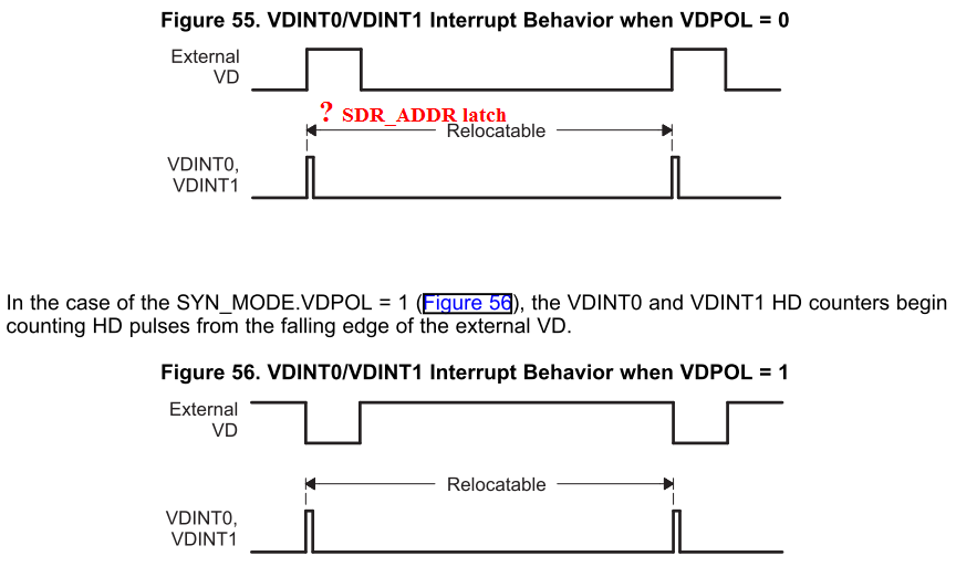
According to 643x VPFE document SPRU977a, page 89, Fig.55 VDINT0/VDINT1 Interrupt Behavior when VDPOL = 0, VPFE interrupt


  1. VDINT0
  2. VDINT1

are generated at the rising (in Fig.56 falling) edge of external VD. Therefore if one wants to use either of these two interrupts’ service routine, for example, VDINT0’s ISR, to change SDR_ADDR, when will SDR_ADDR be latched?

I am asking this question because in page 133, SDR_ADDR is said to be “latched by VD”. If we write code to change SDR_ADDR at the beginning of VDINT0’s ISR, so that upon entering it the command of changing SDR_ADDR is immediately issued, when will it be latched?


  1. If it requires only a positive (or negative, in Fig. 56) VD, then the new value of SDR_ADDR will be effectively latched during the same external VD period.
  2. However, if it can only be latched at the rising (in Fig.56 falling) edge of external VD, then it cannot be latched within the current VD period, but instead has to wait until the next VD, which means one additional frame time has to elapse.

Which is the case? It seems to me a very important question and I welcome anyone who would provide his/her opinion.


Sincerely,
Zheng


  •  

    It will be latched on the next VSYNC, because occurrence of an interrupt indicates that the VSNC has passed. ( in sync with whatever you have mentioned in your point 2)

    May I ask what problem you are trying to solve? because if you analyze the driver, you would get most of the answers for the questions you are asking. Are you trying to write a new driver?.. just curious.


    -Manju


  • Hi All,


    Should I understand "latched by VD" as:


    1. VD is essentially an enabling signal for the latching of many registers (SDR_ADDR, etc.).


    2. The period that VD lasts is defined by VDW of HD and VD Signal Width Register (HD_VD_WID)  in page 128, which is VDW+1 lines. Since every line includes hundreds of pixels and hence lasts in time for hundreds of pixel clocks, and each pixel clock lasts more than 20 CPU clocks (for example, CPU clock rate 600MHz, pixel clock rate 27MHz), therefore

    Length(VD) = (VDW+1) × line = (VDW+1) × (720+) × (CPU clocks per pixel) =  (VDW+1) × (720+) × [ (1/27M ) / (1/600M) ] > (VDW+1) × 720 × 22 > VDW * 15000 (CPU clock cycle)

    So there are at least tens of thousands of CPU clock cycles contained in the period of VD, and of course the said number of rising and falling edge of CPU clock cycles.


    3. When VD is one (when VDPOL=0) these CPU clock cycles are allowed to be used to latch register values (such as SDR_ADDR), and when VD is zero the latching is disabled. When VDPOL=1 the case is the same with only a VD value reversal in the VDPOL=0 case: when VD = 0 these CPU clocks are allowed to latch register values.


    4. Only after we have considered to this microscopic level can we then realize that during each VD period there is such a large number of CPU clock cycles elapsed. Since CPU clock cycles abound within each VD (1 when VDPOL=0, 0 when VDPOL=1), as long as one of these CPU clock cycles effectively latches the register value (SDR_ADDR, etc.), there is no necessity for one to bother considering whether register values are latched on the rising or falling edge of a CPU clock cycle.


    Because of the forgoing discussion, the question in the previous post is answered by:

    Register values are not latched upon to the rising or falling edge of VD, but at the rising or falling edge of one of the large number of CPU clock cycles within the period of VD (1 when VDPOL=0, 0 when VDPOL=1). In which of these CPU clock cycles and at whether the rising or falling edge is determined by the internal operation of the CPU, which is probably not knowable by the programmer and is not relevant to practical use.


    For each of the above points and arguments, are they correct?


    Sincerely,

    Zheng


  • Dear Manju,

    Knowing this is important to the application. Without this knowledge I cannot know whether the new SDR_ADDR value will be latched by the current VD or the next (one frame time's difference). I want to get a sense of certainty.

    Is the driver C or assembly source code? Are they obtainable? If not proprietary, could you provide me a link to them?


    Sincerely,
    Zheng

  • Anonymous
    0 Anonymous in reply to Anonymous

    I think I was wrong on this.


    On page 90, SPRU977a, 643x VPFE User's Guide, the document says that:

    SPRU977a said:

    SDR_ADDR:

    When CCDCFG.VDLC is cleared to 0, written values take effect only at the start of a frame event (rising edge of VD, if SYN_MODE.VDPOL is positive; falling edge of VD, if SYN_MODE.VDPOL is negative).

    When CCDCFG.VDLC is set to 1, written values take effect only at the start of the frame being output to SDRAM (when the input has reached the HORZ_INFO.SPH pixel of the VERT_START.SLVn line of each field).


    So it was not as what I previously thought that register values are latched at edges of CPU clock cycles within VD.


    Just want a confirmation: if VDLC is 1, if I change SDR_ADDR during VD, the next frame will immediately be saved to the new DDR2 memory address?


    Zheng