Other Parts Discussed in Thread: OMAP-L138, OMAPL138
I have a custom board that I am attempting to do an AIS Nand Boot with the RBL, and it's failing to run.
- CCS v 7.0.3
- Compiler Version: 7.4.23 (legacy COFF output format)
- AISgen for D800K008 Bootloader Version 1.9
I programmed in my AIS Image, RESET the chip and hi RUN in CCS (7.0.3).
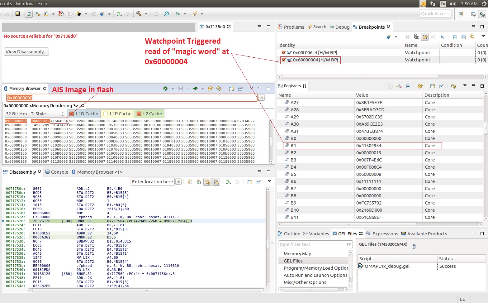
When I pause the execution with my emulator, the chip is still stuck in the RBL memory space (around PC=0x007138D8).
My PLL setting look correct, and some of my PSC registers look correct, however my pinmux don't appear to be configured yet. My flash EMIFA CE2CFG looks correct.
I used the OMAPL1x_debug.gel file to get the results below (and I looked at the registers view in CCS).
NOTE: Since the GEL script did not support floating point numbers and my clock reference is 19.2 MHz, I changed the clock value in the script to 192. That means all PLL clock values are in 10ths of Hz when they are displayed. IE when the script says PLL0_SYSCLK1 is 4032 it actually is 403.2 MHz. I'm not trying to clock the part with a 192 MHz signal :-)
C674X_0: GEL Output:
---------------------------------------------
C674X_0: GEL Output: |             Device Information            |
C674X_0: GEL Output: ---------------------------------------------
C674X_0: GEL Output: DEV_INFO_00 = 0x1B7D102F
C674X_0: GEL Output: DEV_INFO_01 = 0x00000000
C674X_0: GEL Output: DEV_INFO_02 = 0x00000002
C674X_0: GEL Output: DEV_INFO_03 = 0x00000005
C674X_0: GEL Output: DEV_INFO_04 = 0x00000000
C674X_0: GEL Output: DEV_INFO_05 = 0x000003E0
C674X_0: GEL Output: DEV_INFO_06 = 0x00000080
C674X_0: GEL Output: DEV_INFO_07-DEV_INFO_08-DEV_INFO_09-DEV_INFO_10-DEV_INFO_11-DEV_INFO_12 = 0-0-6435593-4-8-28
C674X_0: GEL Output: DEV_INFO_13,DEV_INFO_14,DEV_INFO_15,DEV_INFO_16 = 5,0,0,3887
C674X_0: GEL Output: -----
C674X_0: GEL Output: DEV_INFO_17 = 0x00030003
C674X_0: GEL Output: DEV_INFO_18 = 0x00000000
C674X_0: GEL Output: DEV_INFO_19 =C674X_0: GEL Output: 0C674X_0: GEL Output: 0C674X_0: GEL Output: 0C674X_0: GEL Output: 0C674X_0: GEL Output: 0C674X_0: GEL Output:
C674X_0: GEL Output: -----
C674X_0: GEL Output: DEV_INFO_20 = 0x30303864
C674X_0: GEL Output: DEV_INFO_21 = 0x3830306B
C674X_0: GEL Output: DEV_INFO_22 = 0x00000000
C674X_0: GEL Output: DEV_INFO_23 = 0x00000000
C674X_0: GEL Output: -----
C674X_0: GEL Output: DEV_INFO_24 = 0x0401C008
C674X_0: GEL Output: DEV_INFO_25 = 0x00623309
C674X_0: GEL Output: DEV_INFO_06 = 0x00000080
C674X_0: GEL Output: DEV_INFO_26 = 0x1E5E0005
C674X_0: GEL Output:

C674X_0: GEL Output: ---------------------------------------------
C674X_0: GEL Output: |               BOOTROM Info                |
C674X_0: GEL Output: ---------------------------------------------
C674X_0: GEL Output: ROM ID: d800k008
C674X_0: GEL Output: Silicon Revision 2.1
C674X_0: GEL Output: Boot pins: 2
C674X_0: GEL Output: Boot Mode: NOR
C674X_0: GEL Output:
ROM Status Code: 0x00000000
Description:C674X_0: GEL Output: No error
C674X_0: GEL Output:
Program Counter (PC) = 0x007138CC
C674X_0: GEL Output:
C674X_0: GEL Output: ---------------------------------------------
C674X_0: GEL Output: |              Clock Information             |
C674X_0: GEL Output: ---------------------------------------------
C674X_0: GEL Output:
C674X_0: GEL Output: PLLs configured to utilize 1.2V square wave input.
C674X_0: GEL Output: ASYNC3 = PLL0_SYSCLK2
C674X_0: GEL Output:
C674X_0: GEL Output: NOTE:  All clock frequencies in following PLL sections are based
C674X_0: GEL Output: off OSCIN = 192 MHz.  If that value does not match your hardware
C674X_0: GEL Output: you should change the #define in the top of the gel file, save it,
C674X_0: GEL Output: and then reload.
C674X_0: GEL Output:
C674X_0: GEL Output: ---------------------------------------------
C674X_0: GEL Output: |              PLL0 Information             |
C674X_0: GEL Output: ---------------------------------------------
C674X_0: GEL Output:
C674X_0: GEL Output: PLL0_SYSCLK1 = 4032 MHz
C674X_0: GEL Output: PLL0_SYSCLK2 = 2016 MHz
C674X_0: GEL Output: PLL0_SYSCLK3 = 288 MHz
C674X_0: GEL Output: PLL0_SYSCLK4 = 1008 MHz
C674X_0: GEL Output: PLL0_SYSCLK5 = 1344 MHz
C674X_0: GEL Output: PLL0_SYSCLK6 = 4032 MHz
C674X_0: GEL Output: PLL0_SYSCLK7 = 448 MHz
C674X_0: GEL Output:
C674X_0: GEL Output: ---------------------------------------------
C674X_0: GEL Output: |              PLL1 Information             |
C674X_0: GEL Output: ---------------------------------------------
C674X_0: GEL Output:
C674X_0: GEL Output: PLL1_SYSCLK1 = 2976 MHz
C674X_0: GEL Output: PLL1_SYSCLK2 = 1488 MHz
C674X_0: GEL Output: PLL1_SYSCLK3 = 744 MHz
C674X_0: GEL Output:
C674X_0: GEL Output: ---------------------------------------------
C674X_0: GEL Output: |              PSC0 Information             |
C674X_0: GEL Output: ---------------------------------------------
C674X_0: GEL Output:
C674X_0: GEL Output: State Decoder:
C674X_0: GEL Output:  0 = SwRstDisable (reset asserted, clock off)
C674X_0: GEL Output:  1 = SyncReset (reset assered, clock on)
C674X_0: GEL Output:  2 = Disable (reset de-asserted, clock off)
C674X_0: GEL Output:  3 = Enable (reset de-asserted, clock on)
C674X_0: GEL Output: >3 = Transition in progress
C674X_0: GEL Output:
C674X_0: GEL Output: Module 0:	EDMA3CC (0)        STATE = 3
C674X_0: GEL Output: Module 1:	EDMA3 TC0          STATE = 3
C674X_0: GEL Output: Module 2:	EDMA3 TC1          STATE = 3
C674X_0: GEL Output: Module 3:	EMIFA (BR7)        STATE = 3
C674X_0: GEL Output: Module 4:	SPI 0              STATE = 3
C674X_0: GEL Output: Module 5:	MMC/SD 0           STATE = 3
C674X_0: GEL Output: Module 6:	AINTC              STATE = 3
C674X_0: GEL Output: Module 7:	ARM RAM/ROM        STATE = 3
C674X_0: GEL Output: Module 9:	UART 0             STATE = 3
C674X_0: GEL Output: Module 10:	SCR 0 (BR0/1/2/8)  STATE = 3
C674X_0: GEL Output: Module 11:	SCR 1 (BR4)        STATE = 3
C674X_0: GEL Output: Module 12:	SCR 2 (BR3/5/6)    STATE = 3
C674X_0: GEL Output: Module 13:	PRUSS              STATE = 3
C674X_0: GEL Output: Module 14:	ARM                STATE = 0
C674X_0: GEL Output: Module 15:	DSP                STATE = 3
C674X_0: GEL Output:
C674X_0: GEL Output: ---------------------------------------------
C674X_0: GEL Output: |              PSC1 Information             |
C674X_0: GEL Output: ---------------------------------------------
C674X_0: GEL Output:
C674X_0: GEL Output: State Decoder:
C674X_0: GEL Output:  0 = SwRstDisable (reset asserted, clock off)
C674X_0: GEL Output:  1 = SyncReset (reset assered, clock on)
C674X_0: GEL Output:  2 = Disable (reset de-asserted, clock off)
C674X_0: GEL Output:  3 = Enable (reset de-asserted, clock on)
C674X_0: GEL Output: >3 = Transition in progress
C674X_0: GEL Output:
C674X_0: GEL Output: Module 0:	EDMA3CC (1)        STATE = 0
C674X_0: GEL Output: Module 1:	USB0 (2.0)         STATE = 0
C674X_0: GEL Output: Module 2:	USB1 (1.1)         STATE = 0
C674X_0: GEL Output: Module 3:	GPIO               STATE = 0
C674X_0: GEL Output: Module 4:	UHPI               STATE = 0
C674X_0: GEL Output: Module 5:	EMAC               STATE = 0
C674X_0: GEL Output: Module 6:	DDR2 and SCR F3    STATE = 3
C674X_0: GEL Output: Module 7:	MCASP0 + FIFO      STATE = 0
C674X_0: GEL Output: Module 8:	SATA               STATE = 0
C674X_0: GEL Output: Module 9:	VPIF               STATE = 0
C674X_0: GEL Output: Module 10:	SPI 1              STATE = 0
C674X_0: GEL Output: Module 11:	I2C 1              STATE = 0
C674X_0: GEL Output: Module 12:	UART 1             STATE = 0
C674X_0: GEL Output: Module 13:	UART 2             STATE = 0
C674X_0: GEL Output: Module 14:	MCBSP0 + FIFO      STATE = 0
C674X_0: GEL Output: Module 15:	MCBSP1 + FIFO      STATE = 0
C674X_0: GEL Output: Module 16:	LCDC               STATE = 0
C674X_0: GEL Output: Module 17:	eHRPWM (all)       STATE = 0
C674X_0: GEL Output: Module 18:	MMC/SD 1           STATE = 0
C674X_0: GEL Output: Module 19:	UPP                STATE = 0
C674X_0: GEL Output: Module 20:	eCAP (all)         STATE = 0
C674X_0: GEL Output: Module 21:	EDMA3 TC2          STATE = 0
C674X_0: GEL Output: Module 24:	SCR-F0 Br-F0       STATE = 3
C674X_0: GEL Output: Module 25:	SCR-F1 Br-F1       STATE = 3
C674X_0: GEL Output: Module 26:	SCR-F2 Br-F2       STATE = 3
C674X_0: GEL Output: Module 27:	SCR-F6 Br-F3       STATE = 3
C674X_0: GEL Output: Module 28:	SCR-F7 Br-F4       STATE = 3
C674X_0: GEL Output: Module 29:	SCR-F8 Br-F5       STATE = 3
C674X_0: GEL Output: Module 30:	Br-F7 (DDR Contr)  STATE = 3
C674X_0: GEL Output: Module 31:	L3 RAM, SCR-F4, Br-F6 STATE = 3
When the bootloader is "hung up" i'm able to go to the Memory Browser and grab the AIS image form Flash (saved to a .dat file). I verified the entire image is in Flash, all the sections are accounted for, and the final "Jump and Close" command (0x58535906) reflects the proper _c_init00 address.
The L2RAM which Is supposed to be getting filled with the AIS data, is not getting populated from Flash.
- How do I determine where the RBL is going wrong or more accurately how I'm causing the RBL to "choke"?
- Side Note: I've done something similar on the OMAP-L138, however I used a different flash part. That OMAP-L138 did boot with the Micron PC28F256P30, while the C6748 target uses the Cypress S29GL256S90.