This thread has been locked.

If you have a related question, please click the "Ask a related question" button in the top right corner. The newly created question will be automatically linked to this question.

Linux/DM3730: DSI Escape sequence problem

Part Number: DM3730


Tool/software: Linux

Hello.

I'm working on DM3730 on DSI driver for LCD.

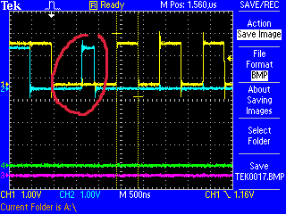
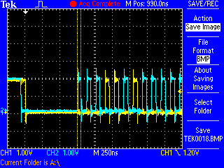
Per MIPI and LCD specfication Low Power clock should have period from 50-75nS.

When I set LP divisor to get this timing in Escape sequence is missing state LP-01.

Also in picture below is sequence with 500ns timing and impuls wide for LP-01 is smaller than other impuls.

In TRM I can not find anything related to settings this.

Is there are any hardware problem or register settings to get this work?

Thanks,

Vojislav

  • Hi Vojislav,

    Could you share register settings which you have done?

    BR
    Tsvetolin Shulev
  • Hi Tsvetolin.

    Thanks for answer.

    Display is 480x800, 24bpp, clk + 2 data lanes.

    I make calculation based on examples from TRM for pixel clk 30MHz.

    Input crystal is 26MHz but based on register settings it is divided by 2.

    Board file settings:

    .phy.dsi.div = {

    .lck_div = 1, /* LCD */

    .pck_div = 4, /* PCD */

    .lp_clk_div = 8, /* LPDIV 8 */

    .regn = 13, /* DSI_PLL_REGN */

    .regm = 360, /* DSI_PLL_REGM */

    .regm3 = 6, /* PLL_CLK1 (M4) */

    .regm4 = 6/* PLL_CLK2 (M5) */

    },

    Clocks:

    - CORE -

    internal clk count              6

    dss_ick         100000000       2

    dss1_alwon_fck  96000000        2

    dss2_alwon_fck  13000000        2

    dss_tv_fck      54000000        0

    dss_96m_fck     96000000        0

    - DSS -

    dpll4_ck 864000000

    dss1_alwon_fclk = 864000000 / 9  = 96000000

    - DISPC -

    dispc fclk source = dsi1_pll_fclk

    fck             120000000      

    lck             120000000       lck div 1

    pck             30000000        pck div 4

    - DSI PLL -

    dsi pll source = dss2_alwon_fclk

    Fint            1000000         regn 13

    CLKIN4DDR       720000000       regm 360

    dsi1_pll_fck    120000000       regm3 6 (on)

    dsi2_pll_fck    120000000       regm4 6 (on)

    - DSI -

    dsi fclk source = dsi2_pll_fclk

    DSI_FCLK        120000000

    DDR_CLK         180000000

    TxByteClkHS     45000000

    LP_CLK          7500000

    VP_CLK          120000000

    VP_PCLK         30000000

    For this settings timings are like in picture below. No escape sequence and first bits are missing

    Also when changing LP_CLK divisor I noticed that after LP10 sequence there is low level on D+/D- pins

    for almost fixed amount of time,  in my case ~800 ns no matter what should be on line. In picture above

    LP01 impuls have smaller width that other impuls. When LP_CLK divisor is set to get 50ns LP_CLK there is no

    LP01 state and also first bits after escape sequence.

    From my point of view it looks like that CPU or DSI controller AND-ing DSI data lines with zero for some

    amount of time but ??? In TRM I can't find anything related to Escape sequence generation and if I'm correct

    that is doing hardware state machine. Only thing that could be programmed are LP_CLK timings and timings

    between Low speed and High speed modes...

    In attach is register dump and debug kernel print.

    If need anything else please ask.

    Once again thanks for help.

    Regards,

    Vojislav

    omapdss MANAGER: omap_dss_mgr_apply(lcd)
    omapdss CORE: restore context
    omapdss CORE: save context
    omapdss OVERLAY: check_overlay 0: (0,0 480x800 -> 480x800) disp (480x800)
    omapdss MANAGER: omap_dss_mgr_apply(lcd)
    omapdss OVERLAY: check_overlay 0: (0,0 480x800 -> 480x800) disp (480x800)
    omapdss CORE: restore context
    omapdss CORE: save context
    omapdss MANAGER: omap_dss_mgr_apply(tv)
    omapdss CORE: restore context
    omapdss CORE: save context
    omapdss DSI: dsi_display_enable
    omapdss CORE: restore context
    omapdss DISPC: xres 0 yres 0
    omapdss DISPC: pck 0
    omapdss DISPC: hsw 1 hfp 1 hbp 1 vsw 1 vfp 0 vbp 0
    omapdss DISPC: hsync 0Hz, vsync 0Hz
    DSI resets: PLL (0) CIO (0) PHY (0, 0, 0, 0)
    omapdss DSI: PLL init
    omapdss DSI: PLL init done
    cinfo->clkin          =13000000
    cinfo->highfreq       =0
    cinfo->fint           =1000000
    cinfo->clkin4ddr      =720000000
    cinfo->dsi1_pll_fclk  =120000000
    cinfo->dsi2_pll_fclk  =120000000
    omapdss DSI: dsi_pll_set_clock_div()
    omapdss DSI: DSI Fint 1000000
    omapdss DSI: clkin (dss2_fck) rate 13000000, highfreq 0
    omapdss DSI: CLKIN4DDR = 2 * 360 / 13 * 13000000 / 1 = 720000000
    omapdss DSI: Data rate on 1 DSI lane 360 Mbps
    omapdss DSI: Clock lane freq 180000000 Hz
    omapdss DSI: regm3 = 6, dsi1_pll_fclk = 120000000
    omapdss DSI: regm4 = 6, dsi2_pll_fclk = 120000000
    omapdss DSI: PLL config done
    omapdss DSI: PLL OK
    omapdss DISPC: lck = 120000000 (1)
    omapdss DISPC: pck = 30000000 (4)
    omapdss DSI: dsi_complexio_init
    omapdss DSI: ths_prepare 15 (83ns), ths_prepare_ths_zero 34 (188ns)
    omapdss DSI: ths_trail 16 (88ns), ths_exit 27 (150ns)
    omapdss DSI: tlpx_half 5 (27ns), tclk_trail 13 (72ns), tclk_zero 47 (261ns)
    omapdss DSI: tclk_prepare 12 (66ns)
    omapdss DSI: dsi_if_enable(1)
    omapdss DSI: dsi_if_enable(0)
    omapdss DSI: dsi_if_enable(1)
    omapdss DSI: dsi_if_enable(0)
    omapdss DSI: CIO init done
    DSI resets: PLL (1) CIO (1) PHY (1, 1, 1, 1)
    omapdss DSI: ddr_clk_pre 23, ddr_clk_post 16
    omapdss DSI: enter_hs_mode_lat 14, exit_hs_mode_lat 14
    omapdss DSI: LP_CLK_DIV 8, LP_CLK 7500000
    DSI resets: PLL (1) CIO (1) PHY (1, 1, 1, 1)
    omapdss DSI: STOP_STATE_COUNTER 4096 ticks (0x1000) = 34133 ns
    omapdss DSI: TA_TO 1048448 ticks (0x1fff x8 x16) = 8737066 ns
    omapdss DSI: LP_RX_TO 524224 ticks (0x1fff x4 x16) = 4368533 ns
    omapdss DSI: HS_TX_TO 524224 ticks (0x1fff x4 x16) = 11649422 ns
    omapdss DSI: dsi_vc_initial_config(0)
    omapdss DSI: dsi_vc_initial_config(1)
    omapdss DSI: dsi_vc_initial_config(2)
    omapdss DSI: dsi_vc_initial_config(3)
    omapdss DSI: dsi_vc_enable channel 0, enable 1
    omapdss DSI: dsi_vc_enable channel 1, enable 1
    omapdss DSI: dsi_vc_enable channel 2, enable 1
    omapdss DSI: dsi_vc_enable channel 3, enable 1
    omapdss DSI: dsi_if_enable(1)
    mmc0: host does not support reading read-only switch. assuming write-enable.
    omapdss DSI: dsi_vc_enable_hs(0, 0)
    omapdss DSI: dsi_vc_enable channel 0, enable 0
    omapdss DSI: dsi_if_enable(0)
    omapdss DSI: dsi_vc_enable channel 0, enable 1
    omapdss DSI: dsi_if_enable(1)
    dsi_vc_send_short(ch1, dt 0x37, b1 0x3, b2 0x0)
    omapdss DSI error: DSI CIO error, cio irqstatus 200000
    DSI CIO IRQ 0x200000: ERRCONTENTIONLP1_1 
    dsi_vc_send_short(ch0, dt 0x6, b1 0x4, b2 0x0)
    omapdss DSI error: DSI CIO error, cio irqstatus 200000
    DSI CIO IRQ 0x200000: ERRCONTENTIONLP1_1 
    omapdss DSI error: DSI CIO error, cio irqstatus 200000
    DSI CIO IRQ 0x200000: ERRCONTENTIONLP1_1 
    mmc0: new SDHC card at address b368
    omapdss DSI error: DSI error, irqstatus 100000
    DSI IRQ: 0x100000: TA_TIMEOUT 
    omapdss DSI error: Failed to receive BTA
    omapdss DSI error: dsi_vc_dcs_read(ch 0, cmd 0x04) failed
    config LCD dsi
    omapdss DSI: dsi_vc_enable_hs(0, 1)
    omapdss DSI: dsi_vc_enable channel 0, enable 0
    omapdss DSI: dsi_if_enable(0)
    omapdss DSI: dsi_vc_enable channel 0, enable 1
    omapdss DSI: dsi_if_enable(1)
    

    DSS_REVISION                        00000020
    DSS_SYSCONFIG                       00000001
    DSS_SYSSTATUS                       00000001
    DSS_IRQSTATUS                       00000000
    DSS_CONTROL                         0000001b
    DSS_SDI_CONTROL                     00000000
    DSS_PLL_CONTROL                     00000000
    DSS_SDI_STATUS                      00000101
    
    DSI_REVISION                        00000010
    DSI_SYSCONFIG                       00000015
    DSI_SYSSTATUS                       00000001
    DSI_IRQSTATUS                       00000000
    DSI_IRQENABLE                       0015c000
    DSI_CTRL                            0108609f
    DSI_COMPLEXIO_CFG1                  2a200312
    DSI_COMPLEXIO_IRQ_STATUS            00000000
    DSI_COMPLEXIO_IRQ_ENABLE            03f01ce7
    DSI_CLK_CTRL                        a0304008
    DSI_TIMING1                         7fff1000
    DSI_TIMING2                         7fff7fff
    DSI_VM_TIMING1                      00000000
    DSI_VM_TIMING2                      00000000
    DSI_VM_TIMING3                      00000000
    DSI_CLK_TIMING                      00001710
    DSI_TX_FIFO_VC_SIZE                 13121110
    DSI_RX_FIFO_VC_SIZE                 13121110
    DSI_COMPLEXIO_CFG2                  00010000
    DSI_RX_FIFO_VC_FULLNESS             00000000
    DSI_VM_TIMING4                      00000000
    DSI_TX_FIFO_VC_EMPTINESS            0000001f
    DSI_VM_TIMING5                      00000000
    DSI_VM_TIMING6                      00000000
    DSI_VM_TIMING7                      000e000e
    DSI_STOPCLK_TIMING                  00000080
    DSI_VC_CTRL(0)                      20808381
    DSI_VC_TE(0)                        00000000
    DSI_VC_LONG_PACKET_HEADER(0)        00000000
    DSI_VC_LONG_PACKET_PAYLOAD(0)       00000000
    DSI_VC_SHORT_PACKET_HEADER(0)       00000000
    DSI_VC_IRQSTATUS(0)                 00000004
    DSI_VC_IRQENABLE(0)                 000000db
    DSI_VC_CTRL(1)                      20800180
    DSI_VC_TE(1)                        00000000
    DSI_VC_LONG_PACKET_HEADER(1)        00000000
    DSI_VC_LONG_PACKET_PAYLOAD(1)       00000000
    DSI_VC_SHORT_PACKET_HEADER(1)       00000000
    DSI_VC_IRQSTATUS(1)                 00000004
    DSI_VC_IRQENABLE(1)                 000000db
    DSI_VC_CTRL(2)                      20800180
    DSI_VC_TE(2)                        00000000
    DSI_VC_LONG_PACKET_HEADER(2)        00000000
    DSI_VC_LONG_PACKET_PAYLOAD(2)       00000000
    DSI_VC_SHORT_PACKET_HEADER(2)       00000000
    DSI_VC_IRQSTATUS(2)                 00000000
    DSI_VC_IRQENABLE(2)                 000000db
    DSI_VC_CTRL(3)                      20800180
    DSI_VC_TE(3)                        00000000
    DSI_VC_LONG_PACKET_HEADER(3)        00000000
    DSI_VC_LONG_PACKET_PAYLOAD(3)       00000000
    DSI_VC_SHORT_PACKET_HEADER(3)       00000000
    DSI_VC_IRQSTATUS(3)                 00000000
    DSI_VC_IRQENABLE(3)                 000000db
    DSI_DSIPHY_CFG0                     0f22101b
    DSI_DSIPHY_CFG1                     42050d2f
    DSI_DSIPHY_CFG2                     b800000c
    DSI_DSIPHY_CFG5                     e7000000
    DSI_PLL_CONTROL                     00000000
    DSI_PLL_STATUS                      00000383
    DSI_PLL_GO                          00000000
    DSI_PLL_CONFIGURATION1              02a96819
    DSI_PLL_CONFIGURATION2              00056000
    
    DISPC_REVISION                      00000030
    DISPC_SYSCONFIG                     00002015
    DISPC_SYSSTATUS                     00000001
    DISPC_IRQSTATUS                     00000000
    DISPC_IRQENABLE                     0000d64f
    DISPC_CONTROL                       00018b08
    DISPC_CONFIG                        00010204
    DISPC_CAPABLE                       000003ff
    DISPC_DEFAULT_COLOR0                00000000
    DISPC_DEFAULT_COLOR1                00000000
    DISPC_TRANS_COLOR0                  00000000
    DISPC_TRANS_COLOR1                  00000000
    DISPC_LINE_STATUS                   000007ff
    DISPC_LINE_NUMBER                   00000000
    DISPC_TIMING_H                      00000000
    DISPC_TIMING_V                      00000000
    DISPC_POL_FREQ                      00000000
    DISPC_DIVISOR                       00010004
    DISPC_GLOBAL_ALPHA                  00000000
    DISPC_SIZE_DIG                      00000000
    DISPC_SIZE_LCD                      07ff07ff
    DISPC_GFX_BA0                       00000000
    DISPC_GFX_BA1                       00000000
    DISPC_GFX_POSITION                  00000000
    DISPC_GFX_SIZE                      00000000
    DISPC_GFX_ATTRIBUTES                00000000
    DISPC_GFX_FIFO_THRESHOLD            03ff03c0
    DISPC_GFX_FIFO_SIZE_STATUS          00000400
    DISPC_GFX_ROW_INC                   00000001
    DISPC_GFX_PIXEL_INC                 00000001
    DISPC_GFX_WINDOW_SKIP               00000000
    DISPC_GFX_TABLE_BA                  00000000
    DISPC_DATA_CYCLE1                   00000000
    DISPC_DATA_CYCLE2                   00000000
    DISPC_DATA_CYCLE3                   00000000
    DISPC_CPR_COEF_R                    00000000
    DISPC_CPR_COEF_G                    00000000
    DISPC_CPR_COEF_B                    00000000
    DISPC_GFX_PRELOAD                   00000100
    DISPC_VID_BA0(0)                    00000000
    DISPC_VID_BA1(0)                    00000000
    DISPC_VID_POSITION(0)               00000000
    DISPC_VID_SIZE(0)                   00000000
    DISPC_VID_ATTRIBUTES(0)             00000000
    DISPC_VID_FIFO_THRESHOLD(0)         03ff03c0
    DISPC_VID_FIFO_SIZE_STATUS(0)       00000400
    DISPC_VID_ROW_INC(0)                00000001
    DISPC_VID_PIXEL_INC(0)              00000001
    DISPC_VID_FIR(0)                    00000000
    DISPC_VID_PICTURE_SIZE(0)           00000000
    DISPC_VID_ACCU0(0)                  00000000
    DISPC_VID_ACCU1(0)                  00000000
    DISPC_VID_BA0(1)                    00000000
    DISPC_VID_BA1(1)                    00000000
    DISPC_VID_POSITION(1)               00000000
    DISPC_VID_SIZE(1)                   00000000
    DISPC_VID_ATTRIBUTES(1)             00000000
    DISPC_VID_FIFO_THRESHOLD(1)         03ff03c0
    DISPC_VID_FIFO_SIZE_STATUS(1)       00000400
    DISPC_VID_ROW_INC(1)                00000001
    DISPC_VID_PIXEL_INC(1)              00000001
    DISPC_VID_FIR(1)                    00000000
    DISPC_VID_PICTURE_SIZE(1)           00000000
    DISPC_VID_ACCU0(1)                  00000000
    DISPC_VID_ACCU1(1)                  00000000
    DISPC_VID_FIR_COEF_H(0, 0)          00000000
    DISPC_VID_FIR_COEF_H(0, 1)          00000000
    DISPC_VID_FIR_COEF_H(0, 2)          00000000
    DISPC_VID_FIR_COEF_H(0, 3)          00000000
    DISPC_VID_FIR_COEF_H(0, 4)          00000000
    DISPC_VID_FIR_COEF_H(0, 5)          00000000
    DISPC_VID_FIR_COEF_H(0, 6)          00000000
    DISPC_VID_FIR_COEF_H(0, 7)          00000000
    DISPC_VID_FIR_COEF_HV(0, 0)         00000000
    DISPC_VID_FIR_COEF_HV(0, 1)         00000000
    DISPC_VID_FIR_COEF_HV(0, 2)         00000000
    DISPC_VID_FIR_COEF_HV(0, 3)         00000000
    DISPC_VID_FIR_COEF_HV(0, 4)         00000000
    DISPC_VID_FIR_COEF_HV(0, 5)         00000000
    DISPC_VID_FIR_COEF_HV(0, 6)         00000000
    DISPC_VID_FIR_COEF_HV(0, 7)         00000000
    DISPC_VID_CONV_COEF(0, 0)           0199012a
    DISPC_VID_CONV_COEF(0, 1)           012a0000
    DISPC_VID_CONV_COEF(0, 2)           079c0730
    DISPC_VID_CONV_COEF(0, 3)           0000012a
    DISPC_VID_CONV_COEF(0, 4)           00000205
    DISPC_VID_FIR_COEF_V(0, 0)          00000000
    DISPC_VID_FIR_COEF_V(0, 1)          00000000
    DISPC_VID_FIR_COEF_V(0, 2)          00000000
    DISPC_VID_FIR_COEF_V(0, 3)          00000000
    DISPC_VID_FIR_COEF_V(0, 4)          00000000
    DISPC_VID_FIR_COEF_V(0, 5)          00000000
    DISPC_VID_FIR_COEF_V(0, 6)          00000000
    DISPC_VID_FIR_COEF_V(0, 7)          00000000
    DISPC_VID_FIR_COEF_H(1, 0)          00000000
    DISPC_VID_FIR_COEF_H(1, 1)          00000000
    DISPC_VID_FIR_COEF_H(1, 2)          00000000
    DISPC_VID_FIR_COEF_H(1, 3)          00000000
    DISPC_VID_FIR_COEF_H(1, 4)          00000000
    DISPC_VID_FIR_COEF_H(1, 5)          00000000
    DISPC_VID_FIR_COEF_H(1, 6)          00000000
    DISPC_VID_FIR_COEF_H(1, 7)          00000000
    DISPC_VID_FIR_COEF_HV(1, 0)         00000000
    DISPC_VID_FIR_COEF_HV(1, 1)         00000000
    DISPC_VID_FIR_COEF_HV(1, 2)         00000000
    DISPC_VID_FIR_COEF_HV(1, 3)         00000000
    DISPC_VID_FIR_COEF_HV(1, 4)         00000000
    DISPC_VID_FIR_COEF_HV(1, 5)         00000000
    DISPC_VID_FIR_COEF_HV(1, 6)         00000000
    DISPC_VID_FIR_COEF_HV(1, 7)         00000000
    DISPC_VID_CONV_COEF(1, 0)           0199012a
    DISPC_VID_CONV_COEF(1, 1)           012a0000
    DISPC_VID_CONV_COEF(1, 2)           079c0730
    DISPC_VID_CONV_COEF(1, 3)           0000012a
    DISPC_VID_CONV_COEF(1, 4)           00000205
    DISPC_VID_FIR_COEF_V(1, 0)          00000000
    DISPC_VID_FIR_COEF_V(1, 1)          00000000
    DISPC_VID_FIR_COEF_V(1, 2)          00000000
    DISPC_VID_FIR_COEF_V(1, 3)          00000000
    DISPC_VID_FIR_COEF_V(1, 4)          00000000
    DISPC_VID_FIR_COEF_V(1, 5)          00000000
    DISPC_VID_FIR_COEF_V(1, 6)          00000000
    DISPC_VID_FIR_COEF_V(1, 7)          00000000
    DISPC_VID_PRELOAD(0)                00000100
    DISPC_VID_PRELOAD(1)                00000100
    
    - CORE -
    internal clk count		6
    dss_ick        	100000000	2
    dss1_alwon_fck 	96000000	2
    dss2_alwon_fck 	13000000	2
    dss_tv_fck     	54000000	0
    dss_96m_fck    	96000000	0
    - DSS -
    dpll4_ck 864000000
    dss1_alwon_fclk = 864000000 / 9  = 96000000
    - DISPC -
    dispc fclk source = dsi1_pll_fclk
    fck		120000000       
    lck		120000000       lck div	1
    pck		30000000        pck div	4
    - DSI PLL -
    dsi pll source = dss2_alwon_fclk
    Fint		1000000         regn 13
    CLKIN4DDR	720000000       regm 360
    dsi1_pll_fck	120000000       regm3 6	(on)
    dsi2_pll_fck	120000000       regm4 6	(on)
    - DSI -
    dsi fclk source = dsi2_pll_fclk
    DSI_FCLK	120000000
    DDR_CLK		180000000
    TxByteClkHS	45000000
    LP_CLK		7500000
    VP_CLK		120000000
    VP_PCLK		30000000
    

  • Hi.

    Any update on this?

    Regards,

    Vojislav

  • Vojislav,

    I'm not founding an issue in the register settings but I found in kernel log some error messages :

    omapdss DSI error: DSI CIO error, cio irqstatus 200000
    DSI CIO IRQ 0x200000: ERRCONTENTIONLP1_1
    dsi_vc_send_short(ch0, dt 0x6, b1 0x4, b2 0x0)
    omapdss DSI error: DSI CIO error, cio irqstatus 200000
    DSI CIO IRQ 0x200000: ERRCONTENTIONLP1_1
    omapdss DSI error: DSI CIO error, cio irqstatus 200000
    DSI CIO IRQ 0x200000: ERRCONTENTIONLP1_1
    mmc0: new SDHC card at address b368
    omapdss DSI error: DSI error, irqstatus 100000
    DSI IRQ: 0x100000: TA_TIMEOUT
    omapdss DSI error: Failed to receive BTA
    omapdss DSI error: dsi_vc_dcs_read(ch 0, cmd 0x04) failed
    config LCD dsi

    The errors starts with DSI CIO IRQ error which is handled in ../drivers/video/omap2/dss/dsi.c file and at the end is detected the issue with synchronization - "Failed to receive BTA" message in ../drivers/video/omap2/dss/dsi.c file which is caused by timeout of wait_for_completion_timeout defined in ../kernel/sched.c file.
    I suspect some hardware related issue.

    BR
    Tsvetolin Shulev
  • Hello Tsvetolin.

    Thanks for answer.

    I know for that error from dmesg and it is caused when panel driver try to read ID from display.

    If I understand correclty, ERRCONTENTIONLP1_1 should mean that there is a bus collison and that hardware try to drive line to high but when readback state is different???

    When you say hardware related issue are you mean on my hardware or to hardware inside of DSP?

    Also same DSP board is used for testing 2 other display in RGB24 mode without problem...

    Timings from scope are when display board is disconnected so there are only signals that come out from DSP.

    Please advice...

    Regards,

    Vojislav

  • Hi.

    Any update?

    Regards,

    Vojislav