Part Number: AM5716
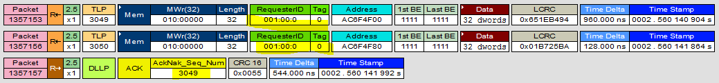
I have an AM571x configured as the PCIe RC with an FPGA endpoint. I am attempting to send a small packet of data from the FPGA to the DSP L2SRAM over PCIe using bus mastered writes. The packet is 292 bytes and requires a number of write transactions to complete, depending on the data payload size. I am encountering issues with parts of the packet not being written correctly into L2SRAM. My initial investigation has led me to believe that I may have a problem with destination address alignment.
1. With inbound data payload sizes of 64 or 128 bytes, parts of the packet are dropped when a single transaction crosses certain memory boundaries. Putting a DATA_ALIGN pragma of 128 bytes on the destination buffer address eliminates this problem.
2. With an inbound data payload size of 256 bytes (the supported maximum), I discovered that no write transaction at this size ever successfully is written into L2SRAM, regardless of what DATA_ALIGN pragma I use (up to a 512 byte alignment requirement). The maximum payload size of the EP FPGA device is 512 bytes and I am not depleting the RC posted header or data credit pools.
According to the AM517x technical reference manual:
"The PCIe controller maximum inbound payload size is 256 Bytes. The PCIe master port burst
maximum length is 16 words (16 x 64-bit data words = 128 Bytes per burst). Hence a 256 Byte
inbound data payload is converted by the PCIe master port to 2 max-sized bursts (128 Byte each)
towards the device L3_MAIN interconnect PCIe slave port which is 128 Byte-burst compatible."
AND
"Non-aligned bursts can be generated - bursts that are not aligned with their own size: a burst-aligned
portion of 2N-bytes aligned burst starts on a byte address multiple of 2N, that is a byte address with the
N LSBs at '0')."
From this language, it is unclear to me what is actually the required destination address alignment of PCIe inbound transactions. Regardless, I do not understand why a 256 byte payload is failing to be written at all.
Thanks for the help,
Sean