This thread has been locked.

If you have a related question, please click the "Ask a related question" button in the top right corner. The newly created question will be automatically linked to this question.

TMS320C6748 USB_VBUS and USB0_DRVVBUS pin functionality

Other Parts Discussed in Thread: TMS320C6748, TPS65070, OMAP-L138

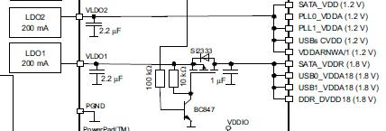
I am now designing a board that uses a TMS320C6748.  I'm wondering if you could answer a question about the processor's USB controller. I am trying to understand the purpose of USB_VBUS and USB0_DRVVBUS. I found this datasheet focusing on the USB controller:

http://focus.ti.com/lit/ug/sprufm9h/sprufm9h.pdf

Sections 2.5 and 2.7 discuss this in detail, but I am still confused about what this pin does. I understand that a host needs to source 0.5A and a device can optionally be powered by this. What I don't understand is the USB controller's role in this. I get that the USB_DRVVBUS pin tells my power supply circuit whether it ought to source power, i.e. whether the DSP is a host. But what is the purpose of USB_VBUS pin? I appreciate any help you can provide.

Thanks again!

Paul

  • USB_DRVVBUS is a signal to control the external 5V supply.

    USB_VBUS is to tell the USB controller if something is connected.  The controller will only monitor the DP/DM lines whenever it sees a valid VBUS level.  If VBUS is not present, the DP/DM lines are ignored.

    --Christina


  • Thank you for responding.  I am still unclear on VBUS, but maybe all I really need to know is this: How should I connect these signals if the USB controller will only be a device (ever a host) and will never draw power from the USB bus?  We're just using it for data communication. 

    Thanks again!
    Paul
  • Paul,

    For device-only, you should connect the USB_VBUS to the USB connector +5 line.  When a host is connected and providing 5V to the device's USB_VBUS signal via the connector, the device should not draw a lot of power because the USB_VBUS is used primarily for sensing the voltage, not for powering the device.

    --Christina

  • Thanks again Christina!  Can you also comment on two other items?

    1.What is the purpose of the FET below?  I understand it delays power from LDO1 until DC-DC #2 is alive, BUT why would we need to do that?  The power sequencing the datasheet recommends is 1.2V --> 1.8V --> 3.3V.  The LDOs by default don't start until DC-DC #3 (1.2V) is up, so why would I want to wait to bring up the 1.8V? 

    2. Am I okay to power the memory controller off DC-DC #2?  The reference design uses LDO #1, but I am worried about exceeding its max current. 

    Thanks again for your assistance!
    Paul
  • PaulSchoenke said:
    What is the purpose of the FET below?  I understand it delays power from LDO1 until DC-DC #2 is alive, BUT why would we need to do that?  The power sequencing the datasheet recommends is 1.2V --> 1.8V --> 3.3V.  The LDOs by default don't start until DC-DC #3 (1.2V) is up, so why would I want to wait to bring up the 1.8V? 

    Can you provide the link to the appnote where you got the image from?  I'll like to see what else is connected.


    PaulSchoenke said:
    Am I okay to power the memory controller off DC-DC #2?  The reference design uses LDO #1, but I am worried about exceeding its max current. 

    The power management page, http://focus.ti.com/analog/docs/refdesignovw.tsp?familyId=64&contentType=2&genContentId=55936, quotes the power very conservatively. You can use the power spreadsheet, http://processors.wiki.ti.com/index.php/C6748/46/42_Power_Consumption_Summary, to determine with finer detail if you are exceeding the max current. 


    --Christina

  • Thanks again Christina!

    The image came from the TPS65070 datasheet, page 72. 

    Thank you for the estimated power requirement table. 

    In my design, all I/O is 3.3V, and it all runs off DC-DC converter #1.  I use DC-DC #2 (1.8V) to power DDR_DVDD18 and a single DDR memory chip to avoid exceeding LDO #1's max current. 

    My main question is the purpose of having a FET delay LDO #1 (1.8V) until DC-DC #2 (strapped for 1.8V in my design) comes up

    I also wonder if there any issues with running DDR memory on a switcher, specifically on DC-DC #2.  I know my power budget is okay.  This question is about noise or any issues apart from maximum current, which will not be a problem.
    I think I might have part of the answer to my sequencing question.  The sequencing we want is 1.2V --> 1.8V --> 3.3V.  I keep saying that at the default configuration TPS65070 won't bring up the LDOs until DC-DC #3 (1.2V) is up.  Therefore the 1.2V comes up before the 1.8V LDO.  What I was forgetting is the other LDO is 1.2V.  We need to make sure LDO #1 (1.8V) does not come up until LDO #2 (1.2V) comes up. 

    Why not gate LDO #1 (1.8V) with LDO #2 (1.2V)?  In other words, why not connect that resistor at the BJT's base to LDO #2's output? Maybe the answer is the transistor would turn on when LDO #2 hit 0.7V, which is too early.  But I could make that same argument if we gate off of the DC-DC #2, as shown in the diagram, b/c the two LDOs and DC-DC #2 are ALL delayed inside TPS65070 until DC-DC #3 comes up (assuming default LDO_CTRL1 and CON_CTRL1 register settings)? 

    I'm hoping someone can explain the thought process behind using that FET.

    Thanks for going over my issue.
    Paul
  • Have you looked at this document, http://focus.ti.com/lit/an/slva371a/slva371a.pdf?  It is similar to the TPS65070 datasheet, but is focused on interfacing it with the OMAP-L138.  Below is taken from page 2 of the document.

    slva371a said:

    If DVDD3318 (DCDC2) is configured for 1.8 V (DEFDCDC2 = low), LDO1 is isolated from the OMAP-L138
    with an external transistor, T2. T2 connects the output of LDO1 to the OMAP-L138 delayed by an external
    circuit consisting of T1, T2, R3, and R4 to meet the correct power-up sequence requirements. If
    DVDD3318 (DCDC2) is configured for 3.3 V (DEFDCDC2 = high), this external delay circuit is not
    required. The LDO output can be directly connected to the OMAP-L138.

    It seems like the original purpose of the delay circuit is to delay LDO1 after DCDC2 (at 1.8V) is powered on.  If DCDC2 is operating at 3.3V, you would want to remove the delay circuit, or else it might break the required power sequence.

    However, my expertise is limited when it comes to power sequencing.  It would be best to create another forum thread for this topic.  Since this thread was originally not related to power sequencing, the visibility for other experts to assist/help is limited.

    --Christina