This thread has been locked.

If you have a related question, please click the "Ask a related question" button in the top right corner. The newly created question will be automatically linked to this question.

AM5728: PCB layout - Guard ring and internal EMC

Part Number: AM5728

Hello,

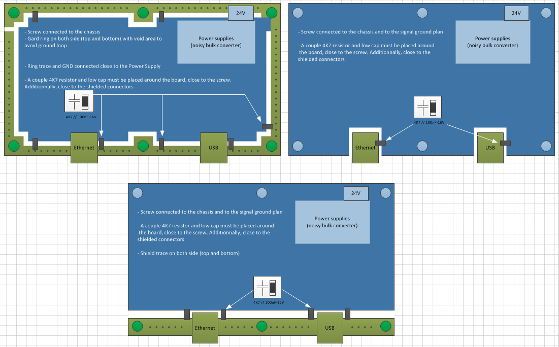
I'm about to build a new board, including an AM5728 and many high speed components  (ethernet, USB3, SATA, wifi...). My concern is about the layout of the board.

I attached a picture with 3 differents topologies of Layout, and I would like to have some feedback to what topology is the best way to prevent any EMC/ESD disturbances.

The first topology with the guard ring is based on the AM57x eval board, but to be honest I'm not very confident with that.

Thanks in advance for your help and advices.

Sylvain.

  • Hi,

    This is a question that cannot be answered generally, as it depends on the environment in which the PCB will be placed. In all cases the guard ring will prevent emissions from the internal layers. Separating the signal GND from chassis will depend on the type of chassis - metal or plastic, and what type of EMI/ESD standard you must meet. It's also a good precaution to provide placeholders for shielding, in case it becomes necessary.
  • Hi,

    just a summary of our application.. the board, including high speed components, will be located into a cabinet with a lot of electronics, and also switching power amplifiers. The boards will communicate with others through oring gigabit ethernet, profinet and USB/HDMI with a touch screen located on the door. The boards will be screwed to a metal chassis (maybe in a box, maybe just screwed on a metal area).

    Usually, the layout of the electronic boards we used to draw looks like the third picture (with a shielded plan screwed to the chassis and a signal ground plan screwed to the same chassis, both isolated and decoupled with capacitors). Maybe such design is enough. But I read a lot of application notes, forum, books talking about guard rings and also the eval boards of the AM57x got one, so...   

  • If ESD is a problem / has to be tested, its good to locate the processor away from the connectors.
    Try to have a minimal distance of 6cm between a connector and the CPU.
  • Yes I agree thank you
  • You can also check section 8 in the AM572x Datasheet SR2.0 Rev. D. Inside you will find links to other useful documents on PCB layout.
  • There is a lot of design rules for interal drawing but nothing about grounding, shielding and guard ring.

    Acutally, the way to improve imunity is a bit confusing for me, a lot of application notes talk about this topic. Most of the time, it recommands to isolate the shielding plan of the signal ground, but some time it recommand to decouple both plan with a 0 ohm, sometimes with 1Meg//100n sometime 4K7//100n, sometime with a ferrite bead, sometime just a capacitor... the worst I saw is 0ohm//100n?!? on TI eval board... I never reach to find a good explanation.
  • You must bear in mind that the TI EVM's are not end products, they are not necessarily tested for EMC/EMI. Please check this document, that comes with every EVM's board files:

    Important Notice for Ref Designs.pdf

  • I agree with you. But it's still confusing :) Do you have any documentation that could help to understand?
  • Our primary business is semi-conductors. We do not have a comprehensive knowledge of system related issues associated with developing a production product. Therefore, we cannot provide guidance on this topic.


    I do not know why the guard ring topology was chosen for this design and cannot justify this approach over other alternatives.


    I can explain why the TI EVM used several 0 ohm resistors when connecting the guard ring to PCB ground. The board was initially designed with a single 0 ohm resistor connecting the guard ring to the PCB ground. However, this resistor was being damaged when the power supply was hot-plugged to the EVM. This occurred because the center contact of the DC barrel connector made contact before the outer contact. The output of the 12 volt DC power supply being used was not isolated which meant the DC ground of the power supply was connected to earth ground through the power cord. A huge inrush of current would flow through this single 0 ohm resistor when the power supply was hot-plugged and the EVM was connected to a PC via a USB cable or monitor via a HDMI cable. Current would flow from the power supply to the board through the center contact of the DC connector, through the EVM circuits and return to the power supply via the single 0 ohm resistor, USB/HDMI cable, and PC power supply connection to earth ground. The inrush of current required to charge the EVM capacitors and power its circuits would exceed the capability of the single 0 ohm resistor and burn it open like a fuse. The EVM was near completion, so we made the minimum number a changes required to resolve this issue. All of the resistors connecting the guard ring to the PCB ground were changed to 0 ohms. The DC barrel connector on the EVM was changed to a model that mates the outer contact before the center contact. The recommended power supply was changed to one that has an isolated output and tuning fork center conductor in the DC barrel connector. It is important the EVM is not allowed to float relative to earth ground, so we provided a large screw terminal connected to the PCB ground which could be used in case the EVM is not connected to earth ground via one of the peripheral cables.


    I wish we could help more with your other questions, but we simply do not have anyone qualified to provide guidance on these topics.


    Regards,
    Paul

  • Hi Paul,

    Thanks a lot for your feedback. At least I understand now why the 0 ohms.

    I think I will start with a chassis plan that group all shielded connectors, decoupled from the signal ground with 1MEG//100nF. The EMC test will validate if capacitors are enough or must be replaced by ferrite bead. The chassis is metalic and connected to the earth, so it make sense for me to connect the screws to the chassis plan. In term of equipotential, I will tied the signal ground to the chassis via screws as well. I hope I will not have any ground loop current between chassis signal ground, capa and chassis plan...

    Thanks for your Help,

    Regards,

    Sylvain.

  • Occasionally we run across system level implementation issues while helping customers. I wanted to mention an issue found several years ago that was related to the USB connector shield connectivity in case you find it useful.

    A PCB assembly was being tested for USB compliance and was failing the low speed and full speed eye diagram tests. After carefully review, we found the test was failing because there was a single transition through the eye. This transition occurred when the bus transitioned from the last data bit transmitted on the bus to SE0 (single-ended-zero) which indicates EOP (end of packet). We finally determined this was happening because the USB connector shield was not connected directly to signal ground. This only occurred when SE0 was driven on the bus because only one of the USB differential signals was toggling from 3.3V to 0V and the energy from the transition was coupling to the shield which reflected from the far end of the cable where the shield was connected to signal ground. This delayed reflection had enough energy to couple back into the USB signal and cross the eye. This issue wasn't seen when the USB signals were driven to opposite states because this doesn't create the unbalanced condition like driving SE0. We were able to resolve the issue by connecting the USB connector shield to the signal ground. In this case, the PCB assembly was an internal development board that wasn't required to pass any radiation emission tests.

    This example shows how you may need to understand many aspects of your system before trying to implement various methods that may or may not help reduce radiated emissions and immunity from ESD.

    Regards,
    Paul