This thread has been locked.

If you have a related question, please click the "Ask a related question" button in the top right corner. The newly created question will be automatically linked to this question.

RTOS/AM5728: Utilize 4GB of DDR

Part Number: AM5728

Tool/software: TI-RTOS

Hello, I've been trying to search the forums and guides on how to configure our project to utilize the 4GB of DDR on our board instead of the default 2GB. After trying to configure our project using the Software Guidelines for EMIF, the two forum posts below, and the EMIF_RegisterConfig tools, I'm still not sure I've gotten it setup correctly.

https://e2e.ti.com/support/legacy_forums/embedded/linux/f/354/t/574408

https://e2e.ti.com/support/processors/f/791/t/680926?tisearch=e2e-sitesearch&keymatch=ddr%20size

The only location in my RTOS project I could find references to the DDR configuration was in the C:\ti\pdk_am57xx_1_0_12\packages\ti\board\src\<customBoard>\<customBoard>_ddr.c file. After modifying the values to match the output from the EMIF Tools spreadsheet, I set the LISA_MAP values to:

    /* Two EMIFs in interleaved mode (2GB in total) */
    /* Reset all LISA MAPs */
    hMampuLsm->MAP_0 = 0x0; //0U;
    hMampuLsm->MAP_1 = 0x0; //0U;
    hMampuLsm->MAP_2 = 0x0; //0U;
    hMampuLsm->MAP_3 = 0x0; //0U;
    hDmmCfg->LISA_MAP[0U] = 0x0; //0U;
    hDmmCfg->LISA_MAP[1U] = 0x0; //0U;
    hDmmCfg->LISA_MAP[2U] = 0x0; //0U;
    hDmmCfg->LISA_MAP[3U] = 0x0; //0U;
    
    /* MA_LISA_MAP_i */
    hMampuLsm->MAP_2 = 0x80740300;
    hMampuLsm->MAP_3 = 0xFF020100;

    /* DMM_LISA_MAP_i */
    hDmmCfg->LISA_MAP[2U] = 0x80740300;
    hDmmCfg->LISA_MAP[3U] = 0xFF020100;

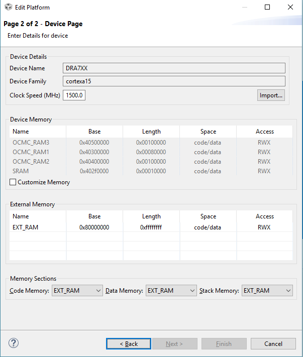
Then I modified the ti.platforms.evmAM572X configuration with the RTSC tools as shown in the screenshot. I've actually tried several different options in this editor, from 1 4GB section, or 2 2GB sections but neither seems to work. From looking at the TRM it looks like with the L3_MAIN Memory Map there is only 2GB available to EMIF1 and 2, but the MPU Memory Map it looks like you should be able to configure 4GB. I'm not sure how all that ties together with the EMIF tool and CCS configuration.

Thanks,

John

  • John,

    TO bring up full DDR range with the SOC, we typically recommend that users firts modify the GEL file provided for the platform and ensure that the DDR is initialized and the SOC cores A15 and DSP can access the full range over the emulator.

    I would break this exercise into four steps:

    Step1 Use EMIF tool to generate GEL configuration for EMIF1 and EMIF2 for the full DDR range.
    www.ti.com/.../sprac36b.pdf

    (Note: SW leveling is not supported so skip Tab2. We support only HW leveling with AM57xx)

    Step2: ensure SOC can access full range in CCS. Open MEmory BRowser from View->Memor y Browser. Open MEmory location in lower 2GB range and perform read write operation. Do the same with address location >2GB that would be on EMIF2. you can also run a DDR diagnostic that reads and writes from entire memory range to check stability of the DDR setup.

    Step3: Apply the changes verified using the GEL file into board library which is target software called by bootloader/application to intiialize DDR without emulator setup for production environment. Update the file pdk_am57xx_x_x_xx\packages\ti\board\src\evmAM572x\evmAM572x_ddr.c

    Step4: Modify the platform memory map and/or linker command file to place code in that range. From software perspective it doesn`t matter that the the DDR is connected to EMIF1 and EMIF2 since it only relies on the address location to place/execute code. Steps you described to modify the platform are correct. you can also do the same by introducing a linker command file to place code in that area.

    Regards,
    Rahul

  • I am trying these steps now, but I feel like this may be a silly question. In Step 2 ensuring access to full range, is the full range 0x00000000 - 0xFFFFFFFF?
  • John,

    No, I meant the full DDR address range + the virtual mapping of the higher 2GB address space. The software configuration of how this is implemented in SPL/Uboot is described here:
    www.ti.com/.../spraca1.pdf

    Let me check internally if we have a GEL implementation of this 4 GB interface with DDR using EMIF1 and EMIF2 that we can share as reference.

    Regards,
    Rahul
  • John Callaway said:
    is the full range 0x00000000 - 0xFFFFFFFF?

    No.

    The Cortex-A15 (which uses 40-bit physical addresses) can access all ram (up to 8GB) via the address range 0x2'000'00'000 - 0x3'fff'ff'fff. As long as you ensure that interleaving is enabled for highmem, i.e. "HIMEM_INTERLEAVE_UN" (bit 8 of the MA_PRIORITY register at 0x482A2000) is set, the first half of this range will be your 4GB ram (except for the 16 MB hole mentioned below).

    The rest of the system (e.g. DMA) uses 32-bit addresses and can only access the 2GB range 0x800'00'000 - 0xfff'ff'fff which is an alias of 0x2'800'00'000 - 0x2'fff'ff'fff. This range actually has configurable mapping to physical ram (via LISA), but the typical LISA setup (which is also what you've shown in your original post) simply maps it to the first 2GB of ram, interleaved across the EMIFs, except for a 16MB "address hole" region at the end (0xff0'00'000 - 0xfff'ff'fff), intended as destination for unused TILER mappings.

    So, for reference, this is what the address space of the Cortex-A15 looks like (assuming highmem interleaving enabled):

      000'00'000 -    7ff'ff'fff = internal memories and peripherals
      800'00'000 -    fff'ff'fff = map via MA_LISA
    1'000'00'000 -  1'fff'ff'fff = <fault>
    2'000'00'000 -  2'7ff'ff'fff = EMIF 0/1  400'00'000 - 7ff'ff'fff
    2'800'00'000 -  2'fff'ff'fff = map via MA_LISA
    3'000'00'000 -  3'7ff'ff'fff = EMIF 0/1  c00'00'000 - fff'ff'fff
    3'800'00'000 -  3'fff'ff'fff = EMIF 0/1  800'00'000 - bff'ff'fff
    4'000'00'000 - ff'fff'ff'fff = <fault>
    

    For other initiators other than the Cortex-A15 it's:

      000'00'000 -    7ff'ff'fff = internal memories and peripherals
      800'00'000 -    fff'ff'fff = map via DMM_LISA
    

    The standard LISA mapping (0x80740300, 0xFF020100) is:

      800'00'000 -    fef'ff'fff = EMIF 0/1  000'00'000 - 3f7'ff'fff
      ff0'00'000 -    fff'ff'fff = <fault>

    And for your 4GB ram configuration, this is how the addresses actually map to DDR3 signals:

    bits  0- 1 = bytelane
    bits  2- 6 = column addr bits 0-4
    bit   7    = emif select
    bits  8-12 = column addr bits 5-9
    bits 13-15 = bank select
    bits 16-30 = row addr bits 0-14
    bit  31    = row addr bit 15 (inverted)
    bit  32    = ignored

    Hope this helps!

  • Thank you so much Matthijs, that clears up a lot of questions I was having about the actual memory layout. When I run our project, I checked and the highmem interleaving is not enabled.

    I think my disconnect is how that addressing is translated to our project with the LISA_MAP. According to the EMIF configuration document "The 2GB DDR base address starts from 0x8000-0000, the higher 2GB address (0x2-0000-0000) for user space that can be used with the ARM ® LPAE feature support.", but I'm not sure how to access that higher address space. The memory browser only works on the 32bit addresses unless I switch to physical, but then I just get "???" for any addresses in the higher range.

  • LISA's main purpose is to allow somewhat flexible routing of the lowmem (0x8000'0000 - 0xFFFF'FFFF) physical address range to the EMIFs, including interleaved across the EMIFs (in 128-, 256-, or 512-byte slices). There's one for the Cortex-A15 (MA_LISA or LSM) and one for the rest of the system (DMM_LISA), and typically you'd program them the same to keep your sanity. It only supports very coarse block-mapping: up to four naturally-aligned blocks of some power-of-two size between 16MB and 2GB.

    The remaining 6GB of physical space only supports two fixed mappings: the interleaved one (256-byte slices) already shown, and the non-interleaved one which is a bit weirder:

    2'000'00'000 - 2'7ff'ff'fff = EMIF 0  400'00'000 - bff'ff'fff
    2'800'00'000 - 2'fff'ff'fff = map via MA_LISA
    3'000'00'000 - 3'7ff'ff'fff = EMIF 1  800'00'000 - fff'ff'fff
    3'800'00'000 - 3'bff'ff'fff = EMIF 0  c00'00'000 - fff'ff'fff
    3'c00'00'000 - 3'fff'ff'fff = EMIF 1  400'00'000 - 7ff'ff'fff

    In both cases the first 1GB of each EMIF is not reachable via these fixed highmem mappings, hence you are expected to map that using LISA.

    These are all physical addresses. As you correctly pointed out, the virtual address space of the cortex-a15 is only 32-bit, so accessing addresses above 0xFFFF'FFFF requires setting up the mmu to perform suitable address mapping. As for the physical browser, CCS has no way of actually performing an access to a physical address. Apparently the physical memory view works by setting up MMU translation on the fly, but it needs to know a suitable physical address to place the translation table. See link for details.

  • Note btw that it is possible to access any part of ram by changing the target of a LISA mapping, effectively creating a "window" into the full ram. This is probably not very practical for real applications, but it's perfectly adequate if you just want to check whether all of the RAM actually works.