This thread has been locked.

If you have a related question, please click the "Ask a related question" button in the top right corner. The newly created question will be automatically linked to this question.

TMS320VC33: the maximum clock frequency for serial port interface if an external clock used

Part Number: TMS320VC33

Hi, 

I have a question about the serial port interface of the TMS320VC33PEG150.

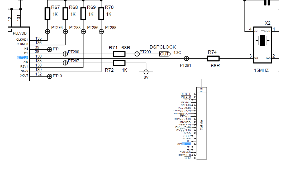
we have a very old product used this chip for many years. and it  use this serial port to receive the Sample data.  the serial port worked in the external clock mode.  and the DSP input clock crystal of 15MHz and PLL output clock= 75Mhz.  recently we want to increase  the frequency of the serial port interface from 1.25Mhz to 5MHz, but find some error in the received data.

i see a description about the  maximum frequency of the serial port in the page 12-42 of datasheet(SPRU031f.pdf): The maximum clock frequency for serial transfers is f(CLKIN)/4 if the internalclock is used and f(CLKIN)/5.2 if an external clock is used. 

but i don'k find where the description of the CLKIN. it means the CLKIN is the pin130 (EXTCLK) ,so the maximum = 15Mhz/5.2=2.84Mhz ?    or the output of the internal PLL, so the maximum = 75Mhz/5.2=14.42Mhz?

could you help to answer this question?

thanks your very much.

B.R.

yong

  • Recently, we are working on a product enhancement project, the DSP processor is TMS320VC33, during debugging, we have found an issue.

    We use a DMA interrupt to copy data from the serial port 0 of the DSP to implement analogue signal sampling.

    The DMA length is set to 16.

    We use two boards, one is responsible for analogue sampling and another is responsible for protection execution. The two boards use a sharedRAM to communicate. The sharedRAM is located in analogue sampling board.

    But during implementation, we found that if the serial port data transfer clock rate is increased, for example, from 1.25Mhz to 2.5MHz, the data we have read from DMA dst address is wrong. And this error always occurred once the two boards write/read shardRAM.

    So is there any link between sharedRAM access and serial port data transfer clock rate.

    Can anyone give me some help? Thanks.

  • I have got some serial communication clock rate limitation in the manual of TMS320VC33. It said that "The maximum clock frequency for serial transfers is f(CLKIN)/4 if the internal clock is used and f(CLKIN)/5.2 if an external clock is used. " What is the CLKIN? Is it the crystal clock?
    With many thanks.
  • Recently, we are working on a product enhancement project, the DSP processor is TMS320VC33, during debugging, we have found an issue.

    We use a DMA interrupt to copy data from the serial port 0 of the DSP to implement analogue signal sampling. The DMA count is set to 16, the DMA source address is set to Serial port 0 receive address, and the DMA destination address is set to a INT32 array with length 16.

    The serial port 0 received data length is 16bits.

    This setting means that in every analogue sample, there are 16 channels, the data length of every channel is 16bits. Everytime, the serial port has received a 16bits data, DMA-coprocessor will move the data to array[0]. Serial port receiving the data of 2nd channel, and then DMA-coprocessor move it to the array[1], and so on.

    We use two boards, one is responsible for analogue sampling and another is responsible for other calculation. The two boards use a sharedRAM to communicate with each other. The sharedRAM is located in analogue sampling board.

    But during implementation, we found that if the serial port data transfer clock rate is increased, for example, from 1.25Mhz to 2.5MHz, the data we have read from DMA destination address is dislocated. For example, the data should have been the third channel, it actually goes to the first channel, the data should have been in the fourth channel, it actually goes to the second channel, and so on...

    This issue becomes serious when the clock rate is increase more, for example. from 1.25MHz to 5MHz (Please refer to attached picture, the CLKR0 is surrounded by a blue box).

    Could anyone give me some help? Thanks.

  • I apologize for the delay in responding to these questions. This is an old device that is not recommended for new designs and this is limited support. I will do my best to help answer what I can.

    For the serial port, looking at the documentation, I believe the CLKIN to be a clock applied to the CLKX0 and/or CLKR0 pins of the DSP. This would allow an external source to control the bit rate of the serial port. The clock source selection is controlled by the Serial-Port Global-Control Register. Bits 6 & 7 control "XCLK SRCE" and "RCLK SRCE" respectively.

  • Have you probed the connections of the serial interface? Do you see the correct data being transmitted?
    Is the data pipe between the ADC, the shared RAM, DMA, Serial port synchronized?
    What is the baseline configuration of CLKR0? How are you modifying it's frequency?
  • Please let me know if you still have questions. For now I'll assume this is resolved.