This thread has been locked.

If you have a related question, please click the "Ask a related question" button in the top right corner. The newly created question will be automatically linked to this question.

Two matters about C55x DSPs' input Clock options.

Other Parts Discussed in Thread: TMS320VC5509A

Hello,

As we know there are two options for system clock and oscillator input. 

  1. External crystal+internal oscillator system
  2. External Clock (+ disabling internal oscillator

There are two matters attracted my attention and I like to discuss them here.

The first subject:

I always use one of these two options in my designs, either an external oscillator like 12 MHz NX3225SA or an oscillator module like a 12 MHz ASDMB as the external clock. Yesterday I was thinking of using both of them at the same time.

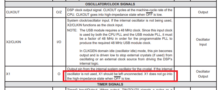
The image above has been taken from the datasheet of TMS3205509A and the image below has been taken from TMS320C5545.

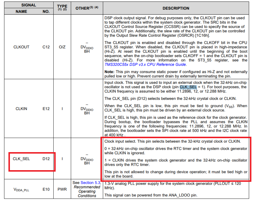
Let's return to the main subject. Imagine that I'm using a TMS320C5545 and I want to use both of external crystal and oscillator module (clock) at the same time. Due to CLK_SEL and by using a simple jumper which can connect this pin to 1.8 v VCC or GND, simply we can switch from external crystal to oscillator module (clock) and vice versa. But what if I want to use e.g. a tMS320VC5509A. This processor is not completely similar with TMS320C5545 and there is not any pin like CLK_SEL which let us switch between two options of clock input?

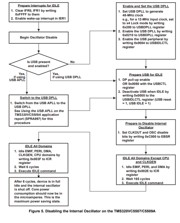
For example, when we are using an external crystal both X1 and X2/CLK are connected to the crystal's pins and simultaneously the output terminal of the clock oscillator is connected to X2/CLK. Again I have the idea for disabling the internal oscillator of DSP when I want to switch from crystal option to oscillator clock. The image below.

But the question in my mind is about the red box in the first image describing the status of X1 when the internal oscillator is disabled. It says the X1 terminal in this mode should be unconnected, while as I mentioned before I'd like to use crystal and oscillator at the same time so X1 is could not be unconnected. Therefore what would happen? 

But the second matter:

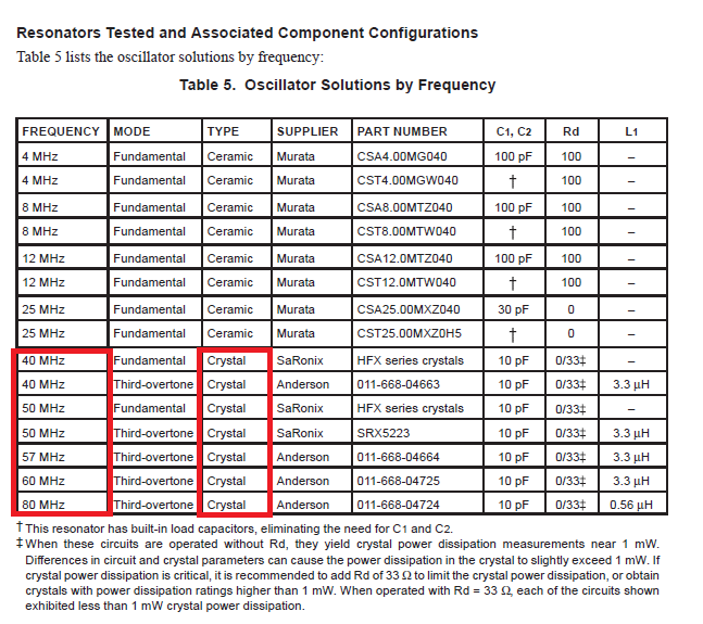
I was reading a document under the name SPRA054 (Use of the TMS320C5x Internal Oscillator With External Crystals or Ceramic Resonators Application Report) that a strange statement got my attention. Take the image below and the red box.

Ok, it's clear enough to understand the limitation of the internal oscillator for operation above 80 MHz. The matter is to carry out an operation in the maximum frequency of CPU (e.g. for TMS320VC5509A is 200 MHz)

The first condition is to ser CVDD to 1.6 v.

The second condition is to generate the clock with this frequency. There are three methods to do this:

  1. External clock input with capability to divide the clock frequency by two

  2. External clock input to an on-board phase-locked loop (PLL) which can multiply the clock
    frequency by one, two, three, four, five, or nine
  3. Internal clock generation from an on-board oscillator with no external clock necessary

From the red box in the last image we can conclude that the method number 3 is not sufficient to reach 200 MHz of operating frequency. There are two other remaining ways, one is to use a 400 MHz oscillator clock and the second way is to use 40 MHz oscillators and with the help of on-board PLL we can reach 200 MHz by multiplying the input clock by five. The second method is my usual technique whenever I need to have an operation at the maximum frequency (200 MHz). 
Is there anyother suggestion?

Regards,
Hossein

  • Hi Hossein,

    By using both at the same time, do you mean populating both options on a board and choosing between one or the other with a jumper? You cannot use both at the same time, or switch from one to the other without putting the DSP in a RESET state (or powered off). That is not supported.

    On the C5545...

    There are 3 clock inputs: CLKIN, USB, and RTC. Of those CLKIN and RTC can be used as the source for SYSCLK.

    CLK_SEL selects either the 32.768kHz RTC oscillator or an exernal clock source to the CLKIN pin as the clock source for the system clock. You cannot alter the state of CLK_SEL while DSP is powered and out of reset - you must either power off the DSP or hold it in reset before changing the state of CLK_SEL.
    When the CLK_SEL pin is low (RTC selected), the CLKIN pin should be tied to ground (VSS). When CLK_SEL is high (CLKIN selected), the CLKIN pin should be driven by an external clock source like a clock oscillator.

    USB: USB_MXO / USB_MXI can be clocked either by a crystal or external clock source.
    When using an external 12-MHz oscillator, the external oscillator clock signal should be connected to the USB_MXI pin and the amplitude of the oscillator clock signal must meet the VIH requirement. The USB_MXO is left unconnected and the USB_VSSOSC signal is connected to board ground (VSS).

    The RTC_XI and RTC_XO pins should be connected to a crystal so the internal oscillator can generate a clock. If you require the use of the RTC, then RTC must be clocked regardless of the CLK_SEL state. In all cases CVDDRTC must be supplied (not by an on-chip LDO). In theory, you could use an external clock source (like a clock oscillator) with the RTC. In that case, the clock signal should be connected to RTC_XI and meet the VIL/VIH for the CVDDRTC voltage domain, and the RTC_XO pin should then be left floating.


    On the C5509A...

    X1 and X2/CLKIN clocks both System Clock and the USB subsystem so its frequency must be a factor of 48 MHz (if USB is required). Similar to the USB oscillator on the C5545, a crystal may be connected between X1(XO) and X2(XI) or X2/CLKIN may be driven by an external clock source like a clock oscillator while X1 is left floating.
    The C5509A has the additional feature of driving out on X1 when the system is in an idle state with the PLL disabled. In that case, X1 can drive low to either stop the crystal from oscillating or to an Enable/Disable pin of the clock oscillator.

    If you were to attach both a crystal and an external oscillator to the X2/CLKIN pins (assuming the external oscillator is not active when the crystal oscillator is used), I would have concerns about the crystal circuit working properly. It is sensitive to capacitive loading and may not begin to oscillate. I have deeper concerns if both are active at the same time. Avoid this. When the external clock oscillator is selected, I think a jumper (depopulated 0-ohms or other logic) should be used to disconnect X1 from the crystal and to ground that side of the crystal (this recommendation is unverified).

    The purpose of Figure 5 is to document the procedure for entering the lowest-power idle state (with the internal oscillator disabled). It is not intended as a method for switching from crystal oscillator to external clock source.

    Table 5-1. Recommended Crystal Parameters offers recommendations for crystals upto 20MHz.

    Table 5-2. CLKIN Timing Requirements limits the input clock of CLKIN upto 50MHz. For frequencies beyond 50MHz, you are expected to use the on-chip PLL to multiply the input frequency to the target system clock frequency.

    Even with the crystal or oscillator runnign < 20MHz, the PLL and SYSCLK can reach their maximum speeds (with limitations integer multiplier and divider factors considered).

    Hope this helps,
    Mark
  • Hi Mark,

    First of all, let me thank you for taking the time in writing this reply. 

    Mark Mckeown said:


    By using both at the same time, do you mean populating both options on a board and choosing between one or the other with a jumper? You cannot use both at the same time, or switch from one to the other without putting the DSP in a RESET state (or powered off). That is not supported.

    Yes, your guess is true. I didn't mean I wanted to use both simultaneously but rather using with a jumper or sth similar to it.

    Mark Mckeown said:


    On the C5545...

    There are 3 clock inputs: CLKIN, USB, and RTC. Of those CLKIN and RTC can be used as the source for SYSCLK.

    CLK_SEL selects either the 32.768kHz RTC oscillator or an exernal clock source to the CLKIN pin as the clock source for the system clock. You cannot alter the state of CLK_SEL while DSP is powered and out of reset - you must either power off the DSP or hold it in reset before changing the state of CLK_SEL.
    When the CLK_SEL pin is low (RTC selected), the CLKIN pin should be tied to ground (VSS). When CLK_SEL is high (CLKIN selected), the CLKIN pin should be driven by an external clock source like a clock oscillator.

    USB: USB_MXO / USB_MXI can be clocked either by a crystal or external clock source.
    When using an external 12-MHz oscillator, the external oscillator clock signal should be connected to the USB_MXI pin and the amplitude of the oscillator clock signal must meet the VIH requirement. The USB_MXO is left unconnected and the USB_VSSOSC signal is connected to board ground (VSS).

    The RTC_XI and RTC_XO pins should be connected to a crystal so the internal oscillator can generate a clock. If you require the use of the RTC, then RTC must be clocked regardless of the CLK_SEL state. In all cases CVDDRTC must be supplied (not by an on-chip LDO). In theory, you could use an external clock source (like a clock oscillator) with the RTC. In that case, the clock signal should be connected to RTC_XI and meet the VIL/VIH for the CVDDRTC voltage domain, and the RTC_XO pin should then be left floating.

    Thanks. Everything is clear.

    Mark Mckeown said:


    The purpose of Figure 5 is to document the procedure for entering the lowest-power idle state (with the internal oscillator disabled). It is not intended as a method for switching from crystal oscillator to external clock source.

    That's completely true. Thanks.

    Mark Mckeown said:


    Table 5-1. Recommended Crystal Parameters offers recommendations for crystals upto 20MHz.

    Your are completely true and Table 5-1 does not offer recommendations for crystals upto 20MHz, but what do you say about the image below captured from  SPRA054, October 1995.

    Mark Mckeown said:


    Table 5-2. CLKIN Timing Requirements limits the input clock of CLKIN upto 50MHz. For frequencies beyond 50MHz, you are expected to use the on-chip PLL to multiply the input frequency to the target system clock frequency.

    Even with the crystal or oscillator runnign < 20MHz, the PLL and SYSCLK can reach their maximum speeds (with limitations integer multiplier and divider factors considered).

    So the only way to reach the maximum speed of CPU is to use an external clock oscillator (or even crystal ) and PLL. In conclusion, there is not any way to reach the maximum system clock frequency. I myself have been using a 40MHz oscillator and after multiplying by 5 the system frequency at the maximum rate is produced.

    Your response is one the most complete replies I've ever received from anyone on e2e.ti.com and this shows your patience and responsibility. 

    Regards,
    Hossein

  • Hi @Mark Mckeown,
    What is your answer to the issue related to the last picture in my last message?

    Your reply:
    "Table 5-1. Recommended Crystal Parameters offers recommendations for crystals upto 20MHz."

    my following issue:
    "Your are completely true and Table 5-1 does not offer recommendations for crystals upto 20MHz, but what do you say about the image below captured from SPRA054, October 1995."

    Regards,
    Hossein
  • Hi Hossein,

    The device datasheet supersedes any other document or advice. In the VC5509A datasheet, Table 5-1. Recommended Crystal Parameters specifies a maximum Frequency of 20MHz. Table 5-2. CLKIN Timing Requirements limits the input clock of CLKIN upto 50MHz.
    You can use the PLL to reach maximum frequency, but there may be a tradeoff in attaining the maximum peripheral frequency if the integer, power of two dividers do not allow dividing the max SYSCLK to the max peripheral frequency.

    SPRA054 is an old appnote that refers to TMS320C5x User’s Guide (literature number SPRU056).

    I believe it is referring to the TMS320C5x processor, which was in production before the TMS320C55xx family members came along - including 'VC5509A and 'VC5507, C5545, etc.

    Refer to this publication - TIs DSP History in Die Form, by Gene Frantz (I think you will enjoy it).

    cnx.org/.../TI-s-DSP-History-in-Die-Form
    Link: cnx.org/.../TIs-DSP-History-in-Die-Form
    Gene Frantz, TI's DSP History in Die Form. OpenStax CNX. Oct 4, 2012 cnx.org/.../c8c1d893-3ede-4248-90a6-84730dbee6b4@1.
    © Oct 4, 2012 Gene Frantz. Textbook content produced by Gene Frantz is licensed under a Creative Commons Attribution License 3.0 license.

    Regards,
    Mark

  • Hi Mark,

    Mark Mckeown said:

    Hi Hossein,

    The device datasheet supersedes any other document or advice.

    This briefly clarifies the issue.

    Thanks,

    Mark Mckeown said:

    Refer to this publication - TIs DSP History in Die Form, by Gene Frantz (I think you will enjoy it).

    cnx.org/.../TI-s-DSP-History-in-Die-Form
    Link: cnx.org/.../TIs-DSP-History-in-Die-Form
    Gene Frantz, TI's DSP History in Die Form. OpenStax CNX. Oct 4, 2012 cnx.org/.../c8c1d893-3ede-4248-90a6-84730dbee6b4@1.
    © Oct 4, 2012 Gene Frantz. Textbook content produced by Gene Frantz is licensed under a Creative Commons Attribution License 3.0 license.

    Thank you for this enjoyable historical publication.

    Regards,
    Hossein