This thread has been locked.

If you have a related question, please click the "Ask a related question" button in the top right corner. The newly created question will be automatically linked to this question.

RTOS/AM5728: configuration of GPMC in 16-bit address/data multiplexed mode

Part Number: AM5728

Tool/software: TI-RTOS

Hi

I'm braking my head on GPMC configuration in 16-bit address/data multiplexed mode.

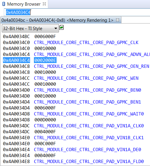
GPMC_ADVN_ALE is not coming out of CPU !!!

1. I set bits 9:8 MUXADDDATA to 0x2 as suggested.

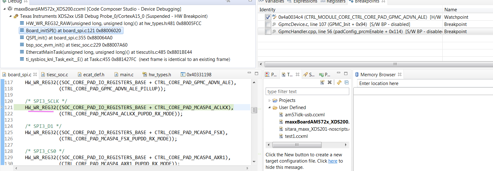
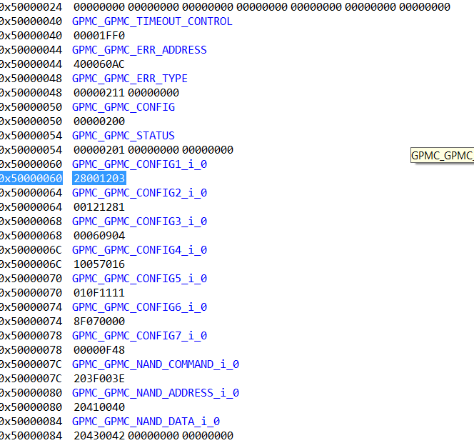
2. Traced down to assembly that I write 0x28001200 to  0x50000060

3. Pin configuration

HW_WR_REG32(CSL_MPU_CORE_PAD_IO_REGISTERS_REGS+CSL_CONTROL_CORE_PAD_IO_PAD_GPMC_ADVN_ALE,0x10000);

4. CS control registers 0..6

0x28001200,
0x80881,
0x60594,
0x10857096,
0x10F1111,
0x8F0000,
0x00000f48, 

What else do I miss?

Thanks

Rasty

:

  • Hi Rasty,

    ADVAADMUXWROFFTIME and ADVAADMUXRDOFFTIME are set to 0 while ADVAADMUXONTIME is set to 1. This is invalid.
    When using MUX mode, you must program these bit fields for the first ADV phase. If two phases are not required, then you may program the MUX bit fields to match ADVONTIME, ADVWROFFTIME, and ADVRDOFFTIME.

    Refer to section 15.4.4.9.3 of the TRM...
    "GPMC_CONFIG3_i[6:4] ADVAADMUXONTIME, GPMC_CONFIG3_i[26:24] ADVAADMUXRDOFFTIME, and GPMC_CONFIG3_i[30:28] ADVAADMUXWROFFTIME parameters have the same functions as ADVONTIME, ADVRDOFFTIME, and ADVWROFFTIME, but apply to the first address phase in the AADmultiplexed protocol. The user must ensure that ADVAADMUXxxOFFTIME is programmed to a value less than or equal to ADVxxOFFTIME. Functionality in AAD-multiplexed mode is undefined if the settings do not comply with this requirement. ADVAADMUXxxOFFTIME can be programmed to the same value as ADVONTIME if no high nADV pulse is needed between the two AAD-multiplexed address phases, which is the typical case in synchronous mode. In this configuration, nADV is kept low until it reaches the correct ADVxxOFFTIME."

    Similar advice applies to the OE control signal.

    Are other GPMC signals toggling as expected?
    To trigger the ADVn signal to toggle with CS0 low, you must make an access to the GPMC memory map with a write or read from an address in the CS0 space - address 0x00000000 will map to CS0.

    I see also that ADVEXTRADELAY is set, enabling an extra half-GPMC_FCLK cycle before driving the ADV signals as programmed in GPMC_CONFIG3_0. This is fine, as long as timings are satisfied for the FPGA/memory.

    Your pad configuration looks okay to me...
    HW_WR_REG32(CSL_MPU_CORE_PAD_IO_REGISTERS_REGS+CSL_CONTROL_CORE_PAD_IO_PAD_GPMC_ADVN_ALE,0x00010000);
    - muxmode set to 0 - 0x0: gpmc_advn_ale routed to the pad
    - Disabled weak Pull Up/Down --> in our examples, we keep weak pull enabled, Pull Up is selected
    - Receive mode is disabled --> in our examples, we keep Receive mode is enabled (sometimes necessary when pad loopback signaling is used, but I don't think it is necessarey for ADVn)

    Are you developing in CCS? You can hit a breakpoint in your code, and check the registers with the register window or memory window at (0x4A0034C4 for CONTROL_CORE_PAD_IO_PAD_GPMC_ADVN_ALE).

    Hope this helps,
    Mark
  • Hi Mark,

    I played with many different values, without success.

    We do not use AAD, just AD. There 2 sets of fields in control registers -  for AAD and AD. Are AAD fields are relevant if I use AD mode? shall I take care about AAD fields?

    Is it possible to get an example of any AD setup that works? I can continue from there.

    Best regards

    Rasty

  • Hi Rasty,

    I have gotten your GPMC register settings running on my AM572 GPEVM.

    Looking at the register window in your last post, the CTRL_CORE_PAD_GPMC_ADVN_ALE register has bits 3:0 GPMC_OEN_REN_MUXMODE = 0xE gpio2_24 instead of 0x0: gpmc_oen_ren.

    Check the line where you write to this register. I use the below setting:
    HW_WR_REG32(
    CSL_MPU_CORE_PAD_IO_REGISTERS_REGS+CSL_CONTROL_CORE_PAD_IO_PAD_GPMC_ADVN_ALE,
    0x00060000);

    One more point I should make is that the AM5728 datasheet supports a maximum GPMC_CLK of 266MHz / 3 = 88.67MHz. To satisfy this requirement, you need to use a GPMCFCLKDIVIDER = 0x2 (divide by 3) and latch synchronous signals with this 88.67MHz clock. To meet setup and hold times of the FPGA, you may need to launch the control signals ALE, WE, OE on different GPMC_FCLK cycles so that they align with the divide-by-3 GPMC_CLK.

    With the divide by 3, the register settings look like this:
    { 0x28001202, 0x00080881, 0x00060594,
    0x10857096, 0x010F1111, 0x008F0000,
    0x00000f48}

    If you need more GPMC_FCLK cycles than the 31 for each control signal OFFTIME, then the TIMEPARAGRANULARITY setting may be used to increment the counters by 1 after 2 FCLK cycles instead of 1 FCLK cycle.

    I am testing GPMC with 32-bit acceses like below. Each 32-bit access gets split into 2 16-bit accesses by the GPMC.

    volatile uint32_t * GPMC0 = (volatile uint32_t*) 0x08000000;
    volatile uint32_t * GPMC1 = (volatile uint32_t*) 0x08000004;
    volatile uint32_t * GPMC2 = (volatile uint32_t*) 0x08000008;
    volatile uint32_t * GPMC3 = (volatile uint32_t*) 0x0800000C;
    ...
    while(1) {

    var0 = *GPMC0;
    var0 = *GPMC1;
    var0 = *GPMC2;
    var0 = *GPMC3;

    *GPMC0 = 0xFFFFFFFF;
    *GPMC1 = 0x55555555;
    *GPMC2 = 0x00000000;
    *GPMC3 = 0xAAAAAAAA;
    }

    Hope this helps,
    Mark
  • Hi Mark

    First of all THANK YOU VERY MUCH for the help!

    Two things bothers me:

    1. Why pinmux did not generate the value that you suggested - I tried many different values but 0x60000?

    2. AND THE Real-problem was that setup of GPMC_ADVN_ALE was overwritten by EtherCAT QSPI setup, I found this with hardware breakpoint. I double checked that GPMC_ADVN_ALE on "AM572X Industrial EVM" does not not go anywhere except Expansion connector and did not expect such a surprise! 

    I'd appreciate a reference to some quick guide that allows me to check pinmux output, why 0x60000 and not 0x20000 or 0x2000e.

    Best regards

    Rasty

  • Hi Rasty

    On #2

    Can you pinpoint the exact  EtherCAT QSPI setup function that overwrites the gpmc_advn_ale

    Regards

    Mukul 

  • Hi Rasty,

    I am glad you found the place that overwrites CORE_PAD_IO_PAD_GPMC_ADVN_ALE. We're investigating why it happens.

    Regarding 

    Rasty Slutsker said:
    1. Why pinmux did not generate the value that you suggested - I tried many different values but 0x60000?

    The Pin Mux Tool will not allow you to set Rx enable for advn_ale(gpmc_advn_ale), but the register does allow it to be written. There is no point in setting Rx enable for ADVn as it is always an output from GPMC.

    I had copied the 0x60000 value from another line of source code without going through the Pin Mux Tool, but it is a possible value for other pins.

    Take ad15(gpmc_ad15) as an example. In the Pin Mux Tool, check the box for Rx and select Pull-up, and the resulting value is 0x60000

    /* GPMC - gpmc_ad15 on H3 - MyGPMC1 */
    #ifdef GPMC_DEFAULT
    {0x143C, 0x60000, {0x0, 0, 0}, {0x0, 0, 0}, {0x0, 0, 0}},

    Regards,
    Mark

  • Hi Mark,
    Thank you very much for your help. We will need SPI next week - we use all available SPIs.
    Please help us to understand why SPI map overlap with GPMC .


    Best regards
    Rasty
  • Hi Rasty 

    I believe this is simply a porting bug and there should be no dependency on this GPMC signal in SPI init.

    I think you can  remove the GPMC config below for now, and we will be cleaning up the pinmux config for SPI in an upcoming release.


        /* GPIO2_23 */

        HW_WR_REG32((SOC_CORE_PAD_IO_REGISTERS_BASE + CTRL_CORE_PAD_GPMC_ADVN_ALE),

                    (CTRL_CORE_PAD_GPMC_ADVN_ALE_PILLUP));

    Let us know if you see any issues or concerns.
    I will mark this post resolved and if there is some additional issues around SPI usage, please feel free to open another E2E post.

    Regards

    Mukul 

  • Hi Mikul
    I'm not sure that it is correct.
    We need both GPMC and SPI.
    Why configuration of SPI3_CLK "fires" to CTRL_CORE_PAD_GPMC_ADVN_ALE? It is not related.
    I think that you must have some copy-paste mistake in definition of SPI3_CLK (and maybe also other pins in this area).

    Best regards
    Rasty
  • Hi Rasty

    The GPMC pin config in AM572x SPI init is surely not needed as far as I acan tell.

    >> I think that you must have some copy-paste mistake in definition of SPI3_CLK
    We are internally discussing this but it appears - in the SPI init(), we are wrongly doing pinmuxing on AM572x IDK from a AM571x IDK board
    example.

    Will have conclusions next week, but wanted to see if this helps unblock you.
  • Hi Mark

    Write via GPMC works, read does not work.

    Pin mux suggests value 0x50000, but if I look into datasheet (Table 18-1161. CTRL_CORE_PAD_GPMC_AD0)

    I see that bit #18 is responsible for read, which yields 0x40000. Please clarify.

    I tried both 0x50000 and 0x40000 and do not see any data.

    Test:

    I put 1.5kOhm external pullup to one of ADx pints (extension connector).

    I expect to see "1" at the corresponding bit if I read any address of GPMC..

    All signals - CLK , RDe, ALE, CS0 are generated correctly, return value is 0

    Where is my mistake?

    Best regards

    Rasty

  • Hi Rasty

    The pinmux setting for GPMC_AD0 looks correct.
    In my project, 0x00050000 is used for CTRL_CORE_PAD_GPMC_ADn

    Can you hit a breakpoint around the GPMC read and verify it is still set correctly in the CCS Registers view?

    If the pin is floating at a header, then you should be able to control the input state with the weak pull-ups / pull-downs. Those can be enabled with bit 16 of the CTRL_CORE_PAD_GPMC_ADn registers and configured high or low with bit 17.

    Regards,
    Mark
  • Hi Mark,
    Checked with debugger first. Value is 0x50000.
    I tried first with "weak" pullups. Then with external "strong".
    The same result read "0".
    If I reconfigure bus to A/D I see change in data when I read GPMC.
    Thanks
    Rasty
  • Found why it happens
    I set SYNC read in GPMC_CONFIG1
    29 READTYPE Selects the read mode operation RW 0x0
    0x1: Read synchronous

    What does it mean? Sitara expects external clock for read operation?

    Thanks
    Rasty
  • Definitely, SYNC read does not bring data to CPU.
    PAD_IO_PAD_GPMC_CLK is 0x50000
  • Hi Rasty,

    I will try to reproduce this behavior in the lab tomorrow morning. Can you pass along your latest GPMC register settings?

    Regards,
    Mark
  • Hi Mark,

    Please notice that if I set 0x08001203 instead of 0x28001200 to CONFIG1 I get data.

    One bit makes a difference.

    I checked pads configuration with debugger, it is the same as below.

    /*Pad configurations*/
    /*GPMC Data lines AD0-AD15*/
    HW_WR_REG32(CSL_MPU_CORE_PAD_IO_REGISTERS_REGS+CSL_CONTROL_CORE_PAD_IO_PAD_GPMC_AD0,0x00060000);
    HW_WR_REG32(CSL_MPU_CORE_PAD_IO_REGISTERS_REGS+CSL_CONTROL_CORE_PAD_IO_PAD_GPMC_AD1,0x00060000);
    HW_WR_REG32(CSL_MPU_CORE_PAD_IO_REGISTERS_REGS+CSL_CONTROL_CORE_PAD_IO_PAD_GPMC_AD2,0x00060000);
    HW_WR_REG32(CSL_MPU_CORE_PAD_IO_REGISTERS_REGS+CSL_CONTROL_CORE_PAD_IO_PAD_GPMC_AD3,0x00060000);
    HW_WR_REG32(CSL_MPU_CORE_PAD_IO_REGISTERS_REGS+CSL_CONTROL_CORE_PAD_IO_PAD_GPMC_AD4,0x00060000);
    HW_WR_REG32(CSL_MPU_CORE_PAD_IO_REGISTERS_REGS+CSL_CONTROL_CORE_PAD_IO_PAD_GPMC_AD5,0x00060000);
    HW_WR_REG32(CSL_MPU_CORE_PAD_IO_REGISTERS_REGS+CSL_CONTROL_CORE_PAD_IO_PAD_GPMC_AD6,0x00060000);
    HW_WR_REG32(CSL_MPU_CORE_PAD_IO_REGISTERS_REGS+CSL_CONTROL_CORE_PAD_IO_PAD_GPMC_AD7,0x00060000);
    HW_WR_REG32(CSL_MPU_CORE_PAD_IO_REGISTERS_REGS+CSL_CONTROL_CORE_PAD_IO_PAD_GPMC_AD8,0x00060000);
    HW_WR_REG32(CSL_MPU_CORE_PAD_IO_REGISTERS_REGS+CSL_CONTROL_CORE_PAD_IO_PAD_GPMC_AD9,0x00060000);
    HW_WR_REG32(CSL_MPU_CORE_PAD_IO_REGISTERS_REGS+CSL_CONTROL_CORE_PAD_IO_PAD_GPMC_AD10,0x00060000);
    HW_WR_REG32(CSL_MPU_CORE_PAD_IO_REGISTERS_REGS+CSL_CONTROL_CORE_PAD_IO_PAD_GPMC_AD11,0x00060000 );
    HW_WR_REG32(CSL_MPU_CORE_PAD_IO_REGISTERS_REGS+CSL_CONTROL_CORE_PAD_IO_PAD_GPMC_AD12,0x00060000);
    HW_WR_REG32(CSL_MPU_CORE_PAD_IO_REGISTERS_REGS+CSL_CONTROL_CORE_PAD_IO_PAD_GPMC_AD13,0x00060000);
    HW_WR_REG32(CSL_MPU_CORE_PAD_IO_REGISTERS_REGS+CSL_CONTROL_CORE_PAD_IO_PAD_GPMC_AD14,0x00060000);
    HW_WR_REG32(CSL_MPU_CORE_PAD_IO_REGISTERS_REGS+CSL_CONTROL_CORE_PAD_IO_PAD_GPMC_AD15,0x00060000);
    /*GPMC Add lines A0-A27*/
    /*GPMC chip select*/
    HW_WR_REG32(CSL_MPU_CORE_PAD_IO_REGISTERS_REGS+CSL_CONTROL_CORE_PAD_IO_PAD_GPMC_CS0,0x10000);
    /*GPMC control lines*/
    HW_WR_REG32(CSL_MPU_CORE_PAD_IO_REGISTERS_REGS+CSL_CONTROL_CORE_PAD_IO_PAD_GPMC_ADVN_ALE,0x00060000);
    HW_WR_REG32(CSL_MPU_CORE_PAD_IO_REGISTERS_REGS+CSL_CONTROL_CORE_PAD_IO_PAD_GPMC_OEN_REN,0x10000);
    HW_WR_REG32(CSL_MPU_CORE_PAD_IO_REGISTERS_REGS+CSL_CONTROL_CORE_PAD_IO_PAD_GPMC_WEN,0x10000);
    HW_WR_REG32(CSL_MPU_CORE_PAD_IO_REGISTERS_REGS+CSL_CONTROL_CORE_PAD_IO_PAD_GPMC_BEN0,0x10000);
    HW_WR_REG32(CSL_MPU_CORE_PAD_IO_REGISTERS_REGS+CSL_CONTROL_CORE_PAD_IO_PAD_GPMC_WAIT0,0xD0000);
    HW_WR_REG32(CSL_MPU_CORE_PAD_IO_REGISTERS_REGS+CSL_CONTROL_CORE_PAD_IO_PAD_GPMC_CLK,0x50000);

  • Hi Rasty,

    I was just able to get back into the lab and test this. I was able to reproduce the same issue you are seeing with GPMC sync read. I am always receiving 0x0. But when I switch to asynch read, I am reading non-zero data.

    I have a feeling this is related to the two stage synchronous mode of capture using first the external (and divided) GPMC_CLK and then the internal GPMC_FCLK.

    See these rules for synchronous modes. Lets make sure the GPMC register settings are satisfying these rules.

    processors.wiki.ti.com/.../Tips_for_configuring_Sitara_GPMC_registers

    I will be OOO tomorrow, but back in office on Friday to play with the GPMC register settings and see if they are satisfying these rules.

    Let me know if you make any discovery in the mean time.

    Regards,
    Mark
  • Hi Rasty,

    I resolved my issue where GPMC synch read always returns 0's by enabling the RX enable bit for the GPMC_CLK pad... It was being written to twice with the second write disabling the RX enable bit...

    /*GPMC CLK RX enabled*/
    HW_WR_REG32(
    CSL_MPU_CORE_PAD_IO_REGISTERS_REGS+CSL_CONTROL_CORE_PAD_IO_PAD_GPMC_CLK,
    0x00050000);

    Please confirm this is not the problem you see. I think you already did this, but worth trying again.

    Even with your original reg settings (from your above screenshot), I am reading non-zero data with synch mode. But on my board all the data pins are floating (except for the one I tied high for testing).

    GPMC_CONFIG1_0 0x28001203
    GPMC_CONFIG2_0 0x00121281
    GPMC_CONFIG3_0 0x00060904
    GPMC_CONFIG4_0 0x10057016
    GPMC_CONFIG5_0 0x010F1111
    GPMC_CONFIG6_0 0x8F070000
    GPMC_CONFIG7_0 0x00000F48

    I ran those reg settings through a GPMC register checker that I have been working on. And it found some issues for synchronous reads.

    The above register settings failed the following checks...

    * RDCYCLETIME < CSRDOFFTIME

    * (RDCYCLETIME - CLKACTIVATIONTIME) a multiple of (GPMCFCLKDIVIDER + 1)

    * Sync Read: Rule 1. PAGEBURSTACCESSTIME must be a multiple of GPMCFCLKDIVIDER+1

    * Sync Read: Rule 2. (RDCYCLETIME – CLKACTIVATIONTIME) must be a multiple of GPMCFCLKDIVIDER+1

    I was able to tweak the register settings and make it pass all checks.

    Note that I changed the GPMCFCLKDIVIDER divider value of 2 instead of 3 - dividing 266MHz by 3 to be the maximum 88.7MHz at the GPMC_CLK pin.

    Let me know if you require 66.5MHz GPMC_CLK. I can rerun the rule checker with that assumption.

    The resulting "clean" register settings are below. These can probably still be optimized more than this.

    GPMC_CONFIG1_0 0x28001202
    GPMC_CONFIG2_0 0x00121281
    GPMC_CONFIG3_0 0x00060904
    GPMC_CONFIG4_0 0x10057016
    GPMC_CONFIG5_0 0x030F1115
    GPMC_CONFIG6_0 0x8F070000
    GPMC_CONFIG7_0 0x00000F48

    Let me know how it goes. I will be taking some time off starting next week.

    Hope this helps.

    Regards,
    Mark