


Hi everyone,
I have some questions about PLL.
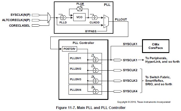
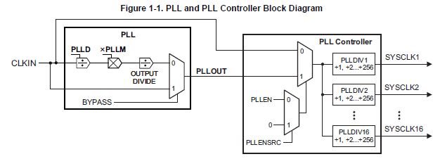
Q1. The following two figures are different. For example, the positions of the multiplier
and divider are different. Which figure is correct?
(SPRS866G : 258page) Figure 11-7. Main PLL and PLL Controller
(SPRUGV2I : 5page) Figure 1-1. PLL and PLL Controller Block Diagram
Q2. How many SYSCLKn does K2H have?
Figure 11-7 shows that it is up to SYSCLK4, but SPRS866G:259page shows that it is up to SYSCLK5.
Q3. Which register is used to set INTERNAL CLOCK DIVIDER(S) and SHARED LOCAL CLOCK DIVIDER for the following?
I'd like to know the registers that set them.
Which function in Figure 11-7 is this divider?

Q4. About the following CLK input of K2H
- SYSCLKP/N (AL3 / AK3)
- ARMCLKP/M (C37 / B37)
- DDR3ACLKP/N (B25 / A25)
- DDR3BCLKP/N (AR38 / AR39)
- SRIOSGMIICLKP/N (AW34 / AW35)
- USBCLKP/N (W2/V2)
- MGTREFCLK0P/N (F6 / E6)
Which PLL register do each correspond to?
DDR3xCLKP/N corresponds to DDR3xPLLCTL0, and ARMCLKP/N corresponds to ARMPLLCTL0.
I do not know the registers corresponding to other clock inputs.
Best regards,
Sasaki

