Hi,
The default configurations for CL and CWL are in ddr3A_setup_1066 function in gel file (C:\ti\ccsv8\ccs_base\emulation\boards\evmk2g\gel\evmk2g_arm.gel):
	// Program BL=0, CL, WR, and PD=1 in the Mode Register 0 (address offset 0x054).
	// All other fields must be left at their default values.
	DDR3A_MR0 = 0x00001830;		//0x00001430; //MM - calculated: 0x00001430, orig: 0x00001420 //-CL - 6, CWL - 5

	// Program DIC, RTT, and TDQS in the Mode Register 1 (address offset 0x058).
	// All other fields must be left at their default values.

	DDR3A_MR1 = 0x00000006;

	// Program Mode Register 2 (address offset 0x05C).
	// Maintaining default values of Program Mode Register 2
	//DDR3A_MR2 = 0x00000018;
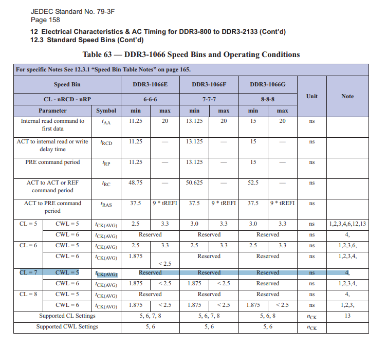
As you see, DDR3A_MR0 is configured as 0x00001830 and DDR3A_MR2 is no update (keeping default value). This means, CL=7 and CWL=5 are configured for 1066Mhz speed bin, but JEDEC suggests this combination should be reserved:
How should we handle this issue ?
Best Regards,
NK


