This thread has been locked.

If you have a related question, please click the "Ask a related question" button in the top right corner. The newly created question will be automatically linked to this question.

DM3730: McBSP receive clock gating

Part Number: DM3730

Hello,

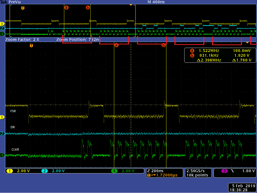
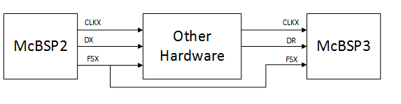
I am using McBSP2 and McBSP3 on a DM3730 processor to send data to and from another hardware device.  My hardware configuration uses McBSP2 as a master to transmit data to the other device, and McBSP3 as a slave to receive data from the other device as per the attached diagram.  Currently the hardware between the McBSPs is gating the clock to McBSP3 so that it is only present when FSX is active - as per the attached scope capture. Ch1 = FSX, Ch2 = CLKX input to McBSP3, and Ch3 = CLKX output from McBSP2.  FSX is configured for active-low, 8-bit frames, 8-cycle pulse width.  Data and Frame sync are sampled on the rising edge.

In this configuration we cannot receive data from McBSP3 - we can transmit any number of bytes from McBSP2, but the McBSP3 DRR register is empty afterwards.  If we connect the free-running McBSP2 clock directly to McBSP3 and make no other HW or SW changes, we can receive data correctly.  Can you help us understand why we are not receiving data?

1. In our configuration McBSP3 never sees FSX inactive (high) on a rising clock edge.  Does the McBSP need to sample frame sync inactive before sampling it active in order to recognize the start of a frame?

2. In our configuration McBSP3 CLKX stops after the end of the frame, and doesn't resume until the start of the next frame.  Are any CLKX pulses required after the end of a frame to move the received data from the shift register to the DRR register?

Thank you for your help,

Steve

  • Hi Steve,

    My very first suggestion is to check McBSP3 clocking related configuration as refer to AM/DM37x Multimedia Device Technical Reference Manual chapter 21 at:
    www.ti.com/.../technicaldocuments
    Pay attention on sections 21.3.2.2.3 McBSP3 Clocks and 21.4.2. about McBSP3 register settings including clock polarity and external clock receiving.
    Also if it is possible compare received clocks in both cases when receive data correctly and when not.

    Regards,
    Tsvetolin Shulev
  • Tsvetolin,

    Thank you for your response. I've looked at these sections of the TRM but I can't find any statement that the McBSP needs to receive a clock edge with frame sync inactive before it can recognize frame sync active. This appears to be the problem but I want to confirm that before making hardware changes.

    In the case where we cannot receive data, the frame sync is asserted active low every time the McBSP receives a clock edge. Can you confirm that the McBSP requires at least one clock edge with frame sync inactive in order to recognize the next frame sync active?

    Thanks,
    Steve
  • Hi Steve,

    Sorry about the delay. Were you able to move forward with this project?

    The master should provide CLKR/CLKX to the McBSP slave before the first frame pulse (during McBSP initialization). Typically the CLK runs continuously once McBSP is initialized.

    Refer to Errata (SPRZ319F) Usage Note 3.5 Undesired McBSP slave mode behavior during reset without CLKR/CLKX
    McBSP port requires two clock cycles of CLKR/CLKX during reset to synchronize the interface configuration. When the McBSP is configured in slave mode, the necessary clock is provided by the other device (the interface master). If the master device does not provide the necessary clock before the first frame pulse, then undesired behavior of the McBSP port will occur since it will only be properly initialized during the first two clock cycles of CLKR/CLKX

    There are other entries in the errata regarding McBSP you should be aware of.

    I am curious if the McBSP is out of sync as a result of this errata. If you provided two additional clock cycles at the end of the frame, would the DRR flag become set?

    Once the receive frame synchronization signal (FSR) transitions to its active state, it is detected on the first internal falling edge of the receivers CLKR (rising edge if polarity inverted).

    Refer also to this post where data alignment was the issue (but they had DRR flag getting set since they were receiving interrupts)...
    e2e.ti.com/.../165965

    Hope this helps,
    Mark
  • What is the configured Data Format?

    For the single word (mono) data shown in the waveform, you might need to use a 1-bit Frame sync pulse instead of a 1-word frame sync pulse (50/50 duty cycle).

    I've asked the designer if the Frame Synch (FSR) requrires a bit clock (CLKR) edge to latch the inactive state and then another CLKR to latch the active state. He might need to know more about the McBSP configuration. Any details you can share are appreciated.

    Regards,
    Mark

  • Hi,

    The designer referred me to the below section from the DM3730 TRM.

    The second paragraph states that the frame sync inputs are sampled using the CLKR_int/CLKX_int clocks. This leads him to conclude that the clocks must be running to sample the frame syncs.

    Regards,
    Mark

  • Mark,

    Thank you for the followup.  I was able to resolve the original issue I posted about by making a hardware change to provide the free-running clock to the slave McBSP.  However, we are having a similar issue with another McBSP receiver where the data pattern is slightly different - see screenshots below.  In this setup the clock to the slave McBSP is gated (I suspect this may be the problem based on the info you provided above from the designer).  The receiving McBSP is configured for slave, falling edge, frame sync active low, 8-bit word length.  Based on TRM 21.4.4.3 and Figure 21-43, I expected the word to begin on the first CLKR falling edge (first picture cursor a) and end on the 8th CLKR falling edge (first picture cursor b) and then continue receiving the next word at the next CLKR falling edge.  I expected the McBSP to ignore the "unexpected receive frame sync" on each CLKR falling edge until the full word has been received.

    What we observe is that the slave McBSP appears to ignore the first two CLKR pulses and begins clocking in data at the next CLKR pulse after the FSR transition (second picture cursor a).  This results in a bit shift in the received data, which I tried to show with the red highlight at the top of each picture.  The data actually in the McBSP receive buffer is shown in the second picture, the data I expected is shown in the first picture.

    We read the errata you provided above and provided several CLKR pulses to the slave McBSP before beginning the data transfer shown in the pictures, but this did not fix the issue.  (Without these extra pulses, the McBSP also did not receive the first full byte of data, so we know that those pulses are getting the slave McBSP in sync.  I didn't see any explicit statements in the TRM that a free-running clock is required in slave mode, although all of the example waveforms do show this.  I am currently testing a hardware change for my second setup that would provide the free-running clock.

    Thanks,

    Steve

  • Hi Steve,

    Its probably due to the lack of a free-running clock again. But its surprising that its the same 2-bit shift that is mentioned in the errata.
    Give the hw change a try, and let me know if you want me to follow up with the designer about it.

    Regards,
    Mark