


Hi,
We development a custom board with OMAP-L138. In the board we put DDR2 memory MT47H128M16RT-25E:C from Micron.
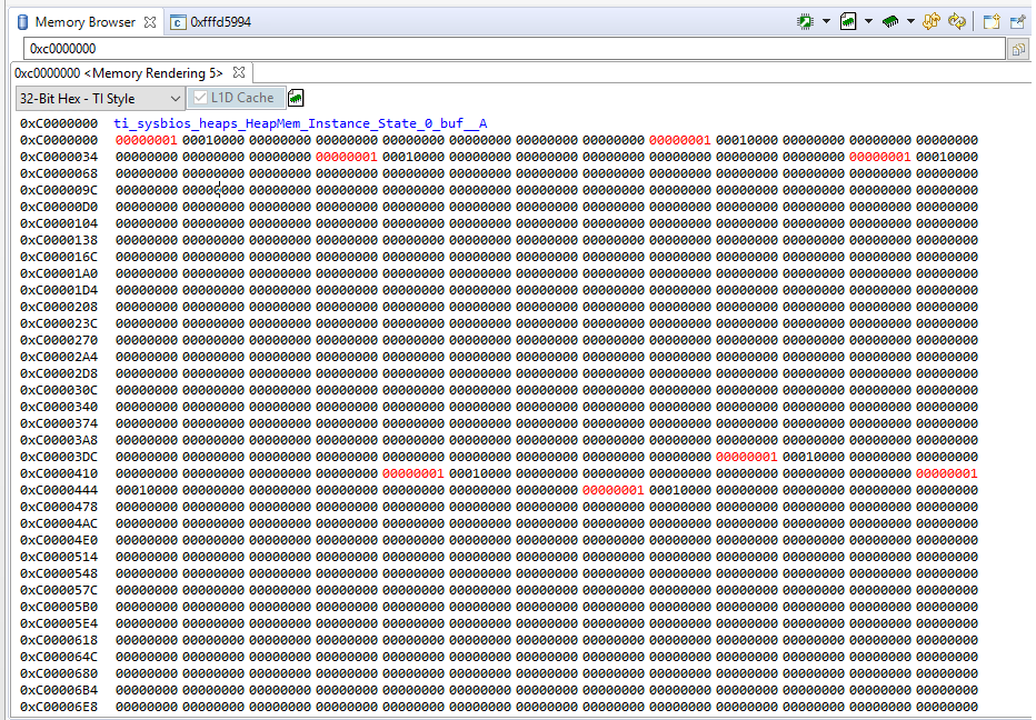
We initialize the DDR in the GEL file according to the datasheet and similarly to the LCDKOMAPL138 board. We succeed to read and write to the memory, but the problem that we facing is that when we write to a single cell in the DDR, multiply cells are changing to the value that we wrote, those cells are not random and have the same offset every time.
In the picture we try to wrote '1' to the first cell but multiply cells has change (appearing in red).
The initialize DDR code we used (with freq = 150 MHz):
#define TRFC 195.0
#define TRP 12.5
#define TRCD 12.5
#define TWR 15.0
#define TRAS 40.0
#define TRC 55.0
#define TRRD 10.0
#define TWTR 7.5
#define TRASMAX 70000.0
#define TREF 7800.0
#define TXP 2
#define TCKE 3
#define TXSNR (TRFC + 10)
#define TXSRD 200
#define TRTP 7.5
#define CL 3

DEVICE_DDRConfig(unsigned int ddr_type, unsigned int freq)
{
    unsigned int j;
    unsigned int tmp_SDCR;
    unsigned int txp;
//    if (TXP > TCKE)
//        txp = TXP - 1;
//    else
//        txp = TCKE - 1;
    // Enable the Clock to EMIFDDR SDRAM
    PSC1_LPSC_enable(PD0, LPSC_DDR);

    // Begin VTP Calibration
    VTPIO_CTL &= ~0x00000040;       // Clear POWERDN
    VTPIO_CTL &= ~0x00000080;       // Clear LOCK
    VTPIO_CTL |=  0x00002000;       // Set CLKRZ in case it was cleared before (VTP looks for CLKRZ edge transition)
    VTPIO_CTL &= ~0x00002000;       // Clear CLKRZ (Use read-modify-write to ensure 1 VTP cycle wait for previous instruction)
    VTPIO_CTL |=  0x00002000;       // Set CLKRZ (Use read-modify-write to ensure 1 VTP cycle wait for previous instruction)

    j = 0;
    // Polling READY bit to see when VTP calibration is done
    while((VTPIO_CTL & 0x00008000) == 0) {
      if( j++ > VTP_TIMEOUT ) {
        GEL_TextOut("\tVTP Ready timeout\n","Output",1,1,1);
        break;
      }
    }

    VTPIO_CTL |= 0x00000080;       // Set LOCK bit for static calibration mode
    VTPIO_CTL |= 0x00000040;       // Set POWERDN bit to power down VTP module
    // End VTP Calibration

    VTPIO_CTL |= 0x00004000;       // Set IOPWRDN to allow powerdown of input receivers when PWRDNEN is set

    // **********************************************************************************************
    // Setting based 1Gb DDR2 Samsung K4T1G164QF-BCF8
    // Config DDR timings
    DRPYC1R     = (0x0               << 8)   |  // Reserved
                  (0x1               << 7)   |  // EXT_STRBEN
                  (0x1               << 6)   |  // PWRDNEN
                  (0x0               << 3)   |  // Reserved
                  (CL + 1               << 0);     // RL
    // DRPYC1R Value = 0x000000C4

    if( DDR_DEBUG ) {
      // Configure EMIF with max timings for more slack
      // Try this if memory is not stable
      DRPYC1R  |=  0x7; // RL
    }

    EMIFDDR_SDCR |= 0x00800000; // Set BOOTUNLOCK

    // Settings depending on DDR2
      tmp_SDCR = (0x0               << 25)  |  // MSDRAMEN
                 (0x1               << 20);    // DDR2EN
      GEL_TextOut("\tUsing DDR2 settings\n","Output",1,1,1);

    EMIFDDR_SDCR = tmp_SDCR                    |  // Settings that change depending on DDR2 or MDDR
                   (EMIFDDR_SDCR & 0xF0000000) |  // Reserved
                   (0x0               << 27)   |  // DDR2TERM1
                   (0x0               << 26)   |  // IBANK_POS
                   (0x0               << 24)   |  // DDRDRIVE1
                   (0x0               << 23)   |  // BOOTUNLOCK
                   (0x0               << 22)   |  // DDR2DDQS
                   (0x0               << 21)   |  // DDR2TERM0
                   (0x0               << 19)   |  // DDRDLL_DIS
                   (0x0               << 18)   |  // DDRDRIVE0
                   (0x1               << 17)   |  // DDREN
                   (0x1               << 16)   |  // SDRAMEN
                   (0x1               << 15)   |  // TIMUNLOCK
                   (0x1               << 14)   |  // NM
                   (0x0               << 12)   |  // Reserved
                   (CL               << 9)    |  // CL
                   (0x0               << 7)    |  // Reserved
                   (0x3               << 4)    |  // IBANK
                   (0x0               << 3)    |  // Reserved
                   (0x2               << 0);      // PAGESIZE

    EMIFDDR_SDCR2   = 0x00000005; // IBANK_POS set to 0 so this register does not apply

    if( DDR_DEBUG ) {
      // Configure EMIF with max timings for more slack
      // Try this if memory is not stable

      EMIFDDR_SDTIMR1 = (0x7F << 25)             |  // tRFC
                        (0x07 << 22)             |  // tRP
                        (0x07 << 19)             |  // tRCD
                        (0x07 << 16)             |  // tWR
                        (0x1F << 11)             |  // tRAS
                        (0x1F << 6)              |  // tRC
                        (0x07 << 3)              |  // tRRD
                        (EMIFDDR_SDTIMR1 & 0x4)  |  // Reserved
                        (0x03 << 0);                // tWTR

      EMIFDDR_SDTIMR2 = (EMIFDDR_SDTIMR2 & 0x80000000)                       |  // Reserved
                        (((unsigned int) ((70000 / 3400) - 0.5))  << 27)   |  // tRASMAX (original 7812.5)
                        (3 - 1                                        << 25)   |  // tXP
                        (0x0                                        << 23)   |  // tODT (Not supported)
                        (0x7F                                       << 16)   |  // tXSNR
                        (0xFF                                       << 8)    |  // tXSRD
                        (0x07                                       << 5)    |  // tRTP (1 Cycle)
                        (0x1F                                       << 0);      // tCKE

      GEL_TextOut("\tDDR Timings Configured for Debug\n","Output",1,1,1);
    }
    else {
      // Let float -> integer truncate handle minus 1; Safer to round up for timings
      EMIFDDR_SDTIMR1 = (((unsigned int) (TRFC * freq / 1000))  << 25)  |  // tRFC
                        (((unsigned int) (TRP * freq / 1000))  << 22)  |  // tRP
                        (((unsigned int) (TRCD * freq / 1000))  << 19)  |  // tRCD
                        (((unsigned int) ( TWR * freq / 1000))  << 16)  |  // tWR
                        (((unsigned int) ( TRAS * freq / 1000))  << 11)  |  // tRAS
                        (((unsigned int) (TRC * freq / 1000))  << 6)   |  // tRC
                        (((unsigned int) ( (4*TRRD + 2*freq/1000)*freq/4000))  << 3)   |  // tRRD
                        (EMIFDDR_SDTIMR1 & 0x4)                          |  // Reserved
                        (((unsigned int) (  TWTR * freq / 1000))  << 0);     // tWTR

      EMIFDDR_SDTIMR2 = (EMIFDDR_SDTIMR2 & 0x80000000)                    |  // Reserved
                        (((unsigned int) ((TRASMAX / TREF)))   << 27)   |  // tRASMAX (original 3400)
                        (TCKE - 1                                        << 25)   |  // tXP
                        (0x0                                     << 23)   |  // tODT (Not supported)
                        (((unsigned int) (TXSNR * freq / 1000))  << 16)   |  // tXSNR (tXSR for mDDR)
                        ((TXSRD - 1)  								 << 8)    |  // tXSRD (tXSR for mDDR)
                        (((unsigned int) (TRTP * freq / 1000))      << 5)    |  // tRTP
                        ((TCKE - 1)                                 << 0);      // tCKE
    }

    EMIFDDR_SDCR    &= ~0x00008000; // Clear TIMUNLOCK

    // Let float -> integer truncate handle RR round-down; Safer to round down for refresh rate
    EMIFDDR_SDRCR   = (0x1                                  << 31)  |  // LPMODEN (Required for LPSC SyncReset/Enable)
                      (0x1                                  << 30)  |  // MCLKSTOPEN (Required for LPSC SyncReset/Enable)
                      (0x0                                  << 24)  |  // Reserved
                      (0x0                                  << 23)  |  // SR_PD
                      (0x0                                  << 16)  |  // Reserved
                      (((unsigned int) (TREF * freq / 1000))  	    << 0);     // RR  (original 7.8125)

    // SyncReset the Clock to EMIFDDR SDRAM
    PSC1_LPSC_SyncReset(PD0, LPSC_DDR);

    // Enable the Clock to EMIFDDR SDRAM
    PSC1_LPSC_enable(PD0, LPSC_DDR);

    // Disable self-refresh
    EMIFDDR_SDRCR &= ~0xC0000000;

    EMIFDDR_PBBPR = 0x20;
}


Any suggestion to what can cause this problem?

