This thread has been locked.

If you have a related question, please click the "Ask a related question" button in the top right corner. The newly created question will be automatically linked to this question.

Impedance reference plane

Hello Community,

I have a board stack of 6 layers, some of which are fully filled planes (plane).

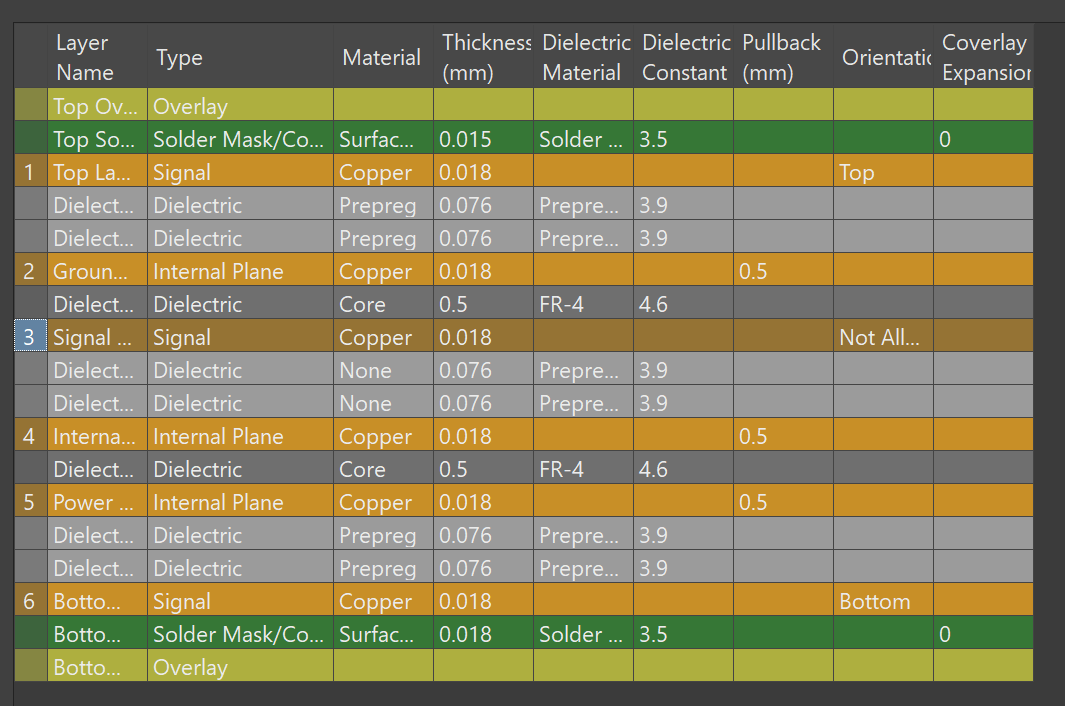
1. Tell me which plane (# 2 or # 4) in my situation is the reference for calculating the impedance for the conductors located on the inner layer (# 3)? And please explain why you think so.
2. Will the split plane, which is NOT a reference, affect the impedance of the adjacent layer?

  • Hi Evgeniy,

    Please find below my inputs, thanks.

    1. I see that Layer2 is a GND layer while Layer4 isn't marked as GND or Signal. I am not sure at what points you are trying to calculate the impedance, maybe you can elaborate more on this.
    2. Since impedance needs to be measured between two different points, I think it will be helpful if I know where exactly are you trying to measure impedance.


    Regards,
    Koteshwar Rao
  • Hi Koteshwar,

    The layer on which the conductors are located whose impedance for me is the sequence number # 3. It is between layers # 2 and # 4, which both represent a plane completely flooded with copper (plane), but for example, connected to different signals (I wrote about this earlier “split plane)”. Plane # 2 is connected to GND, and on plane # 4 it is divided into zones and connected to 3V3, 5V, 12V power supply signals, etc. I am trying to understand whether both planes # 2 and # 4 for layer # 3 are reference points or only one of them? And what is the principle of defining the same supporting plane of these two, if both are simultaneously not supporting?

    P.S. Please look at the first column with sequence numbers, which highlighted the number # 3. The column "Name" can have any name and does not reflect the actual state of connection to this or that signal.

    Thanks for your reply!
  • Hi Evgeniy,

    Thank you elaborating on your question. I am sorry that I still have difficulty in understanding your question completely and accurately.
    The reference point for measuring impedance at any point is something that you would have define based on what impedance you are interesting in. For example, if you want to know impedance of an I/O pin of a device with respect to system GND then system GND is the reference. If you want to measure the impedance between two I/O pins then one of two the pins will become the reference point.

    On a side note, the power supply zones on plane # 4 have different DC voltages of 3.3V, 5V & 12V which I believe are in reference to GND on plane # 2. Since these are DC supplies, they act as short for impedance measurement (as impedance is an AC parameter). Hence, it shouldn't matter whether you reference to GND or power supply zones when measuring impedance on signal traces.

    Like I mentioned in the other E2E post of yours, it will be difficult for us to comment on any generic system level questions that are not tied to any TI device.

    I hope this partly helps you with the information you were looking for. Thank you.


    Regards,
    Koteshwar Rao
  • Hi Koteshwar,

    Well, let's say I need to calculate the impedance of the differential pair (Differential Pair Signal Name: USB1 (USB1_P, USB1_N)) on layer # 3 (Zdiff 90 Ohm), before the GND signal (my voltage source), which is on both planes at the same time # 2 and # 4. (I change the conditions previously mentioned in the example). If I choose plane # 2 as the reference plane, will plane # 4 influence the impedance of layer # 3 because they both belong to GND. Indeed, in my layer stack, plane # 4 has a smaller distance to plane # 3 than plane # 2, as well as a lower dielectric constant?

    Main question:
    Is it possible that when calculating the impedance of USB conductors to GND, when selecting plane # 2 as the reference one, plane # 4 will have a greater effect on layer # 3, being also connected to GND as layer # 2?

    I'm trying to understand how much I need to be careful when placing signals similar to the reference plane on adjacent layers with a conductor for which the impedance is calculated. As some TI notes (I do not remember their number), it is said that even a voltage change on the reference plane can affect the calculated impedance in the case of for example the presence of two signals on the reference plane (for example: 12V, GND) with different values ​​of conductor voltage and passage of them.

  • Hi Evgeniy,

    Thanks for the clarification, it helps me understand your question better.

    If you have the same GND plane spread on both plane # 2 and plane # 4 then based on how these GND zones are overlapping onto the USB signal traces on plane # 3, there will be a capacitance formed. With this I think both plane # 2 & 4 will have an impact on the impedance measurement done on plane # 3 USB signals. This definitely has to be considered into account while calculating the impedance of USB signals on plane # 3.

    If you do have more questions on PCB layout guidelines related to USB devices, I can notify the TI engineer responsible for TI USB products to look into your questions. Let me know, thanks.


    Regards,
    Koteshwar Rao
  • Hi Koteshwar,

    I believe that you answered my questions on the options for the development of the situation that I proposed. I believe that the topic of USB layout and the adaptation of this layout, taking into account the resulting capacity on the overlapping layers, is a separate topic for discussion. Thank you for helping to clarify this issue.

    Good job.