

Hi All,
I would like to ask a question on memory hierarchy speed.
First question:
Qualitatively, we know that the speed of memory devices from high to low is:
(CPU, not a memory device) > register > L1 RAM/Cache > L2 RAM/Cache > DDR2
But quantitatively,
CPU (600MHz for a DM6437) : register : L1 : L2 : DDR2
What are the ratios here? In particular, every CPU cycle takes 1/600M second, what are the required time(s) for every single L1, L2 and DDR2 access?
The above question is flawed in itself since DDR2 uses burst bandwidth, so I should not term the question using “every single access”. To define it more clearly:
- How many clock cycles does it require to load from L1 to register?
- How many clock cycles does it require to load from L2 to register?
- How many clock cycles does it require to load from DDR2 to register?
If anyone would answer this, please do give me quantities as exact as possible for them.
Second question:
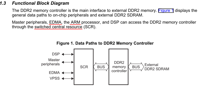
In the figure below appeared on page 8 of SPRU986b, DDR2 controller UG, there is a component called “switched central resource”, which seems to behave like a scheduler for DDR2 accessing attempts. So adding to the above question on DDR2 access clock cycle number, a further complication is that what happens when different components (DSP, Master peripherals, EDMA, VPSS) are competing for DDR2 access? What then will be the
- Maximum
- Minimum
- Average
delay in for CPU’s DDR2 access, in clock cycles? What happens if the configuration makes the shared central resource fully-loaded at most of, say 95%, of the time, or the load’s time average is more than the maximum transferring rate of SCR, i.e., >100%?
Example: VPSS is sending frames at maximum resolution and highest rate, while other peripherals are all working at their maximum output rate?
If this happens, will the CPU just got hang there, waiting wistfully for data? Or does CPU has higher priority than VPSS, EDMA and other peripherals?
A third question is that the introduction of cache further complicated the issue. As a concrete example, suppose that someone allocates all 32KB of L1P as cache. At sometime during the running of the program, 31KB of code has already been copied from DDR2 into L1P to facilitate CPU’s instruction fetching, which up to that point has saved a considerable time for CPU. Then the executes a branch instruction and found that the new branched function has a size of 10KB, which cannot be put into the remaining 32-31=1KB L1P space, what will happen next?
Will the cache management unit (if this is not the name, something similar must exist for cache management) “unload”, or more precisely, “invalidate” all, or some of the used 31KB cache’s memory mapping, and then “upload”, or more precisely, copy branched function’s content L1P? Or will cache management unit just keeps the 31KB copy intact and does not copy the branched function’s 10KB into L1P, but rather let the CPU fetch instructions 1KB at a time, for a total of 10 times?
In cases like this, the actual clock cycle needed for a program’s execution should be very difficult to predict before running, and could differ widely from one’s expectation based on calculation not taking cache into account.
Is this correct? How should one analyze his code's realt-timer performance when cache is enabled then?
Sincerely,
Zheng
