Because of the Thanksgiving holiday in the U.S., TI E2E™ design support forum responses may be delayed from November 25 through December 2. Thank you for your patience.

This thread has been locked.

If you have a related question, please click the "Ask a related question" button in the top right corner. The newly created question will be automatically linked to this question.

Linux/AM3359: GPMC Synchronous - Data is not Reading

Part Number: AM3359

Tool/software: Linux

Dear Sir,

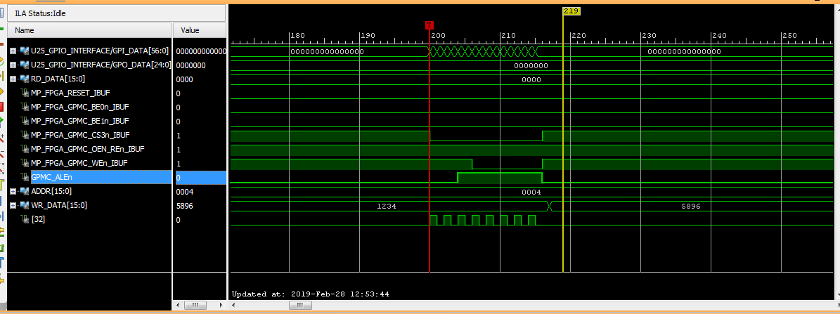
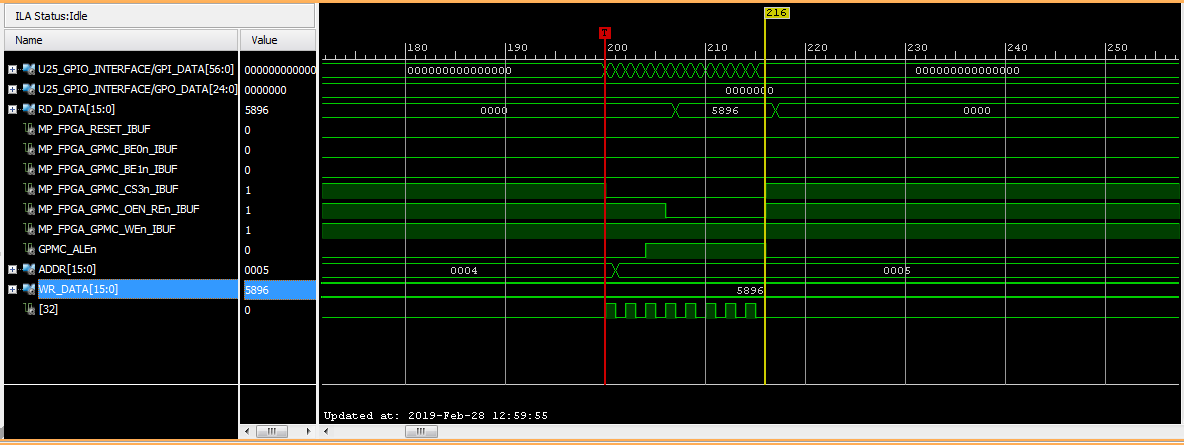
We are trying to enable the GPMC synchronous single  Write / Read operation with external FPGA using NOR protocol.  When we are performing write operation clock is GPMC_CLK is generating and data was written in FPGA but we cant read back the written data. But in asynchronous mode write and read operation is working fine. Please find the attached screen shorts of the wave forms captured in Vivado (FPGA chipscope) for the write ("5896" data is writing in address "4") & Read (data is reading from "5" th address) operation.

The device tree configuration is given below.

                                0x0 (PIN_INPUT_PULLUP | MUX_MODE0)      /* gpmc_ad0.gpmc_ad0 */
                                0x4 (PIN_INPUT_PULLUP | MUX_MODE0)      /* gpmc_ad1.gpmc_ad1 */
                                0x8 (PIN_INPUT_PULLUP | MUX_MODE0)      /* gpmc_ad2.gpmc_ad2 */
                                0xc (PIN_INPUT_PULLUP | MUX_MODE0)      /* gpmc_ad3.gpmc_ad3 */
                                0x10 (PIN_INPUT_PULLUP | MUX_MODE0)     /* gpmc_ad4.gpmc_ad4 */
                                0x14 (PIN_INPUT_PULLUP | MUX_MODE0)     /* gpmc_ad5.gpmc_ad5 */
                                0x18 (PIN_INPUT_PULLUP | MUX_MODE0)     /* gpmc_ad6.gpmc_ad6 */
                                0x1c (PIN_INPUT_PULLUP | MUX_MODE0)     /* gpmc_ad7.gpmc_ad7 */
                                0x70 (PIN_INPUT_PULLUP | MUX_MODE0)     /* gpmc_wait0.gpmc_wait0 */
                                0x7c (PIN_OUTPUT | MUX_MODE0)           /* gpmc_csn0.gpmc_csn0 */
                                0x90 (PIN_OUTPUT | MUX_MODE0)           /* gpmc_advn_ale.gpmc_advn_ale */
                                0x94 (PIN_OUTPUT | MUX_MODE0)           /* gpmc_oen_ren.gpmc_oen_ren */
                                0x98 (PIN_OUTPUT | MUX_MODE0)           /* gpmc_wen.gpmc_wen */
                                0x9c (PIN_OUTPUT | MUX_MODE0)           /* gpmc_be0n_cle.gpmc_be0n_cle */
                                0x88 (PIN_OUTPUT | MUX_MODE0)           /* (T13) gpmc_csn3.gpmc_csn3 */

                                0x24 (PIN_INPUT_PULLUP | MUX_MODE0)       /* gpmc_ad9.gpmc_ad9 */
                                0x28 (PIN_INPUT_PULLUP | MUX_MODE0)       /* gpmc_ad10.gpmc_ad10 */
                                0x2c (PIN_INPUT_PULLUP | MUX_MODE0)       /* gpmc_ad11.gpmc_ad11 */
                                0x30 (PIN_INPUT_PULLUP | MUX_MODE0)       /* gpmc_ad12.gpmc_ad12 */
                                0x34 (PIN_INPUT_PULLUP | MUX_MODE0)       /* gpmc_ad13.gpmc_ad13 */
                                0x38 (PIN_INPUT_PULLUP | MUX_MODE0)       /* gpmc_ad14.gpmc_ad14 */
                                0x3c (PIN_INPUT_PULLUP | MUX_MODE0)       /* gpmc_ad15.gpmc_ad15 */

                                0x74 (PIN_OUTPUT | MUX_MODE2)           /* gpmc_csn0.gpmc_csn0 */

                                0x78 (PIN_OUTPUT | MUX_MODE0)             /* (U18) gpmc_be1n.gpmc_be1n */ /* Added for FPGA */
                                0x8c (PIN_OUTPUT | MUX_MODE0)            /* (V12) gpmc_clk.gpmc_clk */

           ram@3,0 {

                   reg = <3 0x00000000 0x01000000>;
                   bank-width = <2>;
                   gpmc,mux-add-data = <2>;

                   gpmc,device-width = <2>; /* 16-bit devices */
                   gpmc,sync-read;
                   gpmc,sync-write;
                   gpmc,clk-activation-ns = <0>;
                   gpmc,sync-clk-ps = <0>;  /* Minimum clock period for synchronous mode, in picoseconds */

                   gpmc,wait-on-read = "true";
                   gpmc,cs-on-ns = <0>;
                   gpmc,cs-rd-off-ns = <80>;
                   gpmc,cs-wr-off-ns = <80>;
                   gpmc,adv-on-ns = <0>;
                   gpmc,adv-rd-off-ns = <20>;
                   gpmc,adv-wr-off-ns = <20>;
                   gpmc,oe-on-ns = <30>;
                   gpmc,oe-off-ns = <80>;
                   gpmc,we-on-ns = <30>;
                   gpmc,we-off-ns = <80>;
                   gpmc,rd-cycle-ns = <80>;
                   gpmc,wr-cycle-ns = <80>;
                   gpmc,access-ns = <80>;
                   gpmc,page-burst-access-ns = <0>;
                   gpmc,cycle2cycle-samecsen;
                   gpmc,cycle2cycle-delay-ns = <0>;
                   gpmc,wr-data-mux-bus-ns = <30>;
                   gpmc,wr-access-ns = <80>;

           };

In technical reference manual, the GPMC clock pin configuration is mentioned in section 7.1.3.3.9.6 like below.

" When the GPMC is configured for synchronous mode, the GPMC_CLK signal (which is an output)
must also be set as an input in the Pin Mux configuration for the pin. GPMC_CLK is looped back
through the output and input buffers of the corresponding GPMC_CLK pad at the device boundary.
The looped-back clock is used to synchronize the sampling of the memory signals."

How do I configure the clock pin as both output & input ? Currently I have configured as output. Whether I have change the clock pin configuration from output to input in device tree ?

thanks

Mobin P K

Write:

Read:

  • You should change: 0x8c (PIN_OUTPUT | MUX_MODE0) /* (V12) gpmc_clk.gpmc_clk */
    To: 0x8c (PIN_INPUT | MUX_MODE0) /* (V12) gpmc_clk.gpmc_clk */
  • Thanks for your reply.

    After changing the Clock Pin configuration as input. Data is reading the fine.

    thanks
    Mobin
  • Dear Sir,
    We are trying to enable the synchronous burst write and read with 16 words using chip select 5 configuration in the DMA, while performing, Write operation is successfully done but burst read is not working and also burst clock also not generated (only 3 clocks are generated).
    Please find the chip select 5 configurations below and rest of the settings are kept same as mentioned earlier message.

    ram@5,0 {

    reg = <5 0x00000000 0x01000000>;
    bank-width = <2>;
    gpmc,mux-add-data = <2>;
    gpmc,device-width = <2>; /* 16-bit devices */
    gpmc,sync-read;
    gpmc,sync-write;
    gpmc,burst-length = <16>;
    gpmc,burst-wrap;
    gpmc,burst-read;
    gpmc,burst-write;
    gpmc,page-burst-access-ns = <10>;
    gpmc,sync-clk-ps = <0>;
    gpmc,cs-on-ns = <0>;
    gpmc,cs-rd-off-ns = <30>;
    gpmc,cs-wr-off-ns = <30>;
    gpmc,adv-on-ns = <0>;
    gpmc,adv-rd-off-ns = <10>;
    gpmc,adv-wr-off-ns = <10>;
    gpmc,oe-on-ns = <10>;
    gpmc,oe-off-ns = <30>;
    gpmc,we-on-ns = <10>;
    gpmc,we-off-ns = <30>;
    gpmc,rd-cycle-ns = <30>;
    gpmc,wr-cycle-ns = <30>;
    gpmc,access-ns = <30>;
    gpmc,cycle2cycle-samecsen;
    gpmc,cycle2cycle-delay-ns = <10>;
    gpmc,wr-data-mux-bus-ns = <20>;
    gpmc,wr-access-ns = <30>;
    };
    Please suggest me what to be done for synchronous burst read and GPMC_CLK generation as mentioned timing diagram section (7.1.3.3.10.2.2 Synchronous Multiple (Burst) Read (4-, 8-, 16-Word16 Burst With Wraparound Capability).

    Thanks,
    Mobin
  • Hello Mobin,

    Could you please share the register dump for GPMC_CONFIG<1-7>_5?

    Regards,
    Krunal
  • Hello Krunal,
    Thanks for your reply,
    I have added the register dump details for GPMC_CONFIG<1-7> for chip select 5 (The values are in hex format). Please find and provide the solution ASAP.
    GPMC_CONFIG<1> -> 0xF9401200
    GPMC_CONFIG<2> -> 0x00030300
    GPMC_CONFIG<3> -> 0x22010110
    GPMC_CONFIG<4> -> 0x03016311
    GPMC_CONFIG<5> -> 0x01030303
    GPMC_CONFIG<6> -> 0x83020180
    GPMC_CONFIG<7> -> 0x00000f42

    Thank,
    Mobin
  • Hello Mobin,

    It seems like you are violating rules 3 and 4 in the following wiki:


    Please use the following links as references: 


    One recommendation is to increase the Read Cycle Time to satisfy the rules. 

    Regards,

    Krunal

  • Hello Mobin,

    I will be closing the ticket and if you are still experiencing issues, feel free to open the ticket in the future.

    Regards,
    Krunal