Other Parts Discussed in Thread: SYSBIOS
Tool/software: TI-RTOS
I'm studying to access a asynchronous SRAM(16bits,1MByte) on AM437x GPMC.Two examples are used :enet_app_tcpecho, and Nimu_BasicExample_skAM437x_armExampleproject. and its use the same GPMC init function as follow:
void SDKGPMCInit(void)
{
gpmcChipSelTimingParams_t csTimingParams;
gpmcAdvSignalTimingParams_t advSignalTimingParams;
gpmcOeWeSignalTimingParams_t oeWeSignalTimingParams;
gpmcReadAccessTime_t readAccesParams;
gpmcCycle2CycleDelay_t cycleDelayParams;
int32_t status = S_PASS;
// configure the SRAM
GPMCModuleReset(SOC_GPMC_CONFIG_REG);
status = GPMCIsModuleResetDone(SOC_GPMC_CONFIG_REG);
NIMU_log("Board_GPMC reset status [0x%x]\n", status);
status = GPMCGetRevision(SOC_GPMC_CONFIG_REG);
NIMU_log("Board_GPMC version [0x%x]\n", status);
GPMCSetIdleMode(SOC_GPMC_CONFIG_REG, GPMC_IDLE_MODE_NO_IDLE); // no idle
GPMCIntrDisable(SOC_GPMC_CONFIG_REG, GPMC_INTR_MASK_ALL); // disable interrupt
GPMCTimeoutEnable(SOC_GPMC_CONFIG_REG, FALSE); // timout disable
GPMCChipSelEnable(SOC_GPMC_CONFIG_REG, GPMC_CHIP_SEL_1, FALSE); // CS disable
GPMCSetDevType(SOC_GPMC_CONFIG_REG, GPMC_CHIP_SEL_1, GPMC_DEV_TYPE_NOR); // Nor Type
GPMCSetAddrDataMuxType(SOC_GPMC_CONFIG_REG, GPMC_CHIP_SEL_1, GPMC_MUX_TYPE_NONE); // none mux
GPMCSetDevSize(SOC_GPMC_CONFIG_REG, GPMC_CHIP_SEL_1, GPMC_DEV_SIZE_16BIT); // 16bits
GPMCSetAccessMode(SOC_GPMC_CONFIG_REG, GPMC_CHIP_SEL_1, GPMC_OPER_MODE_READ, GPMC_ACCESS_MODE_SINGLE); // single read
GPMCSetAccessMode(SOC_GPMC_CONFIG_REG, GPMC_CHIP_SEL_1, GPMC_OPER_MODE_WRITE, GPMC_ACCESS_MODE_SINGLE); // single write
GPMCSetAccessType(SOC_GPMC_CONFIG_REG, GPMC_CHIP_SEL_1, GPMC_ACCESS_TYPE_ASYNC_READ); // async read
GPMCSetAccessType(SOC_GPMC_CONFIG_REG, GPMC_CHIP_SEL_1, GPMC_ACCESS_TYPE_ASYNC_WRITE); // async write
GPMCSetChipSelBaseAddr(SOC_GPMC_CONFIG_REG, GPMC_CHIP_SEL_1, 0x1000000>>24); // base address=0x1000000
GPMCSetChipSelMaskAddr(SOC_GPMC_CONFIG_REG, GPMC_CHIP_SEL_1, GPMC_MASK_ADDR_16MB); // mask address=0xf, 16MBytes
GPMCSetFclkDivider(SOC_GPMC_CONFIG_REG, GPMC_CHIP_SEL_1, GPMC_FCLK_DIVIDER_1);
GPMCSetTimeParaGranularity(SOC_GPMC_CONFIG_REG, GPMC_CHIP_SEL_1, GPMC_TIME_GRANULARITY_X1);
csTimingParams.chipSelOnTime = 0x00;
csTimingParams.chipSelRdOffTime = 0x07;
csTimingParams.chipSelWrOffTime = 0x07;
csTimingParams.addExtDelay = 0x01;
GPMCChipSelectTimingConfig(SOC_GPMC_CONFIG_REG, GPMC_CHIP_SEL_1, &csTimingParams);
advSignalTimingParams.advOnTime = 0x01;
advSignalTimingParams.advRdOffTime = 0x02;
advSignalTimingParams.advWrOffTime = 0x02;
advSignalTimingParams.addExtDelay = 0x01;
advSignalTimingParams.advAadMuxOnTime = 0x01;
advSignalTimingParams.advAadMuxRdOffTime = 0x02;
advSignalTimingParams.advAadMuxWrOffTime = 0x02;
GPMCAdvSignalTimingConfig(SOC_GPMC_CONFIG_REG, GPMC_CHIP_SEL_1, &advSignalTimingParams);
oeWeSignalTimingParams.oeOnTime = 0x01;
oeWeSignalTimingParams.oeOffTime = 0x06;
oeWeSignalTimingParams.addExtDelay = 0x01;
oeWeSignalTimingParams.writeEnableOnTime = 0x00;
oeWeSignalTimingParams.writeEnableOffTime = 0x06;
oeWeSignalTimingParams.oeAadMuxOffTime = 0x00;
oeWeSignalTimingParams.oeAadMuxOnTime = 0x00;
GPMCWeOeSignalTimingConfig(SOC_GPMC_CONFIG_REG, GPMC_CHIP_SEL_1, &oeWeSignalTimingParams);
readAccesParams.readAccessTime = 0x06;
readAccesParams.readCycleTime = 0x07;
readAccesParams.writeCycleTime = 0x07;
readAccesParams.pageBurstAccessTime = 0x07;
GPMCReadAccessTimingConfig(SOC_GPMC_CONFIG_REG, GPMC_CHIP_SEL_1, &readAccesParams);
GPMCWriteAccessTimingConfig(SOC_GPMC_CONFIG_REG, GPMC_CHIP_SEL_1, 0x06, 0x00);
cycleDelayParams.cycle2CycleDelay = 0x01;
cycleDelayParams.cycleDelayDiffChipSel = 0x01;
cycleDelayParams.cycleDelaySameChipSel = 0x01;
cycleDelayParams.busTurnAroundTime = 0x01;
GPMCCycleDelayTimingConfig(SOC_GPMC_CONFIG_REG, GPMC_CHIP_SEL_1, &cycleDelayParams);
GPMCChipSelEnable(SOC_GPMC_CONFIG_REG, GPMC_CHIP_SEL_1, TRUE); // CS enable
return;
}
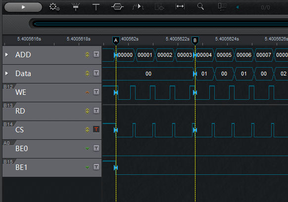
and I use a type uint64_t variable to perform continuous read and write operations.
but I find that there is no time delay between two read or write operations in the example enet_app_tcpecho, while there is about 300ns time delay between two read or write operations in the example Nimu_BasicExample_skAM437x_armExampleproject. ,
I wonder if it's because these two examples call different MMU initializing function.(MMUConfigAndEnable() and CACHEEnable(CACHE_IDCACHE, CACHE_INNER_OUTER) in the enet_app_tcpecho,SDKMMUInit(applMmuEntries) in the Nimu_BasicExample_skAM437x_armExampleproject)
pdk_am437x_1_0_10, sysbios_ind_sdk_2.1.0.1
CCS7
What's the difference between MMU and cache initialization in these two examples? Why do SRAM access timing differ?