This thread has been locked.

If you have a related question, please click the "Ask a related question" button in the top right corner. The newly created question will be automatically linked to this question.

TMS320C6748: TMS320C6748

Part Number: TMS320C6748

Hi Friends,

I am using TMS320C6748 LCDK Dev Kit Rev A7A. I have using the starterware support from ti .On the example codes

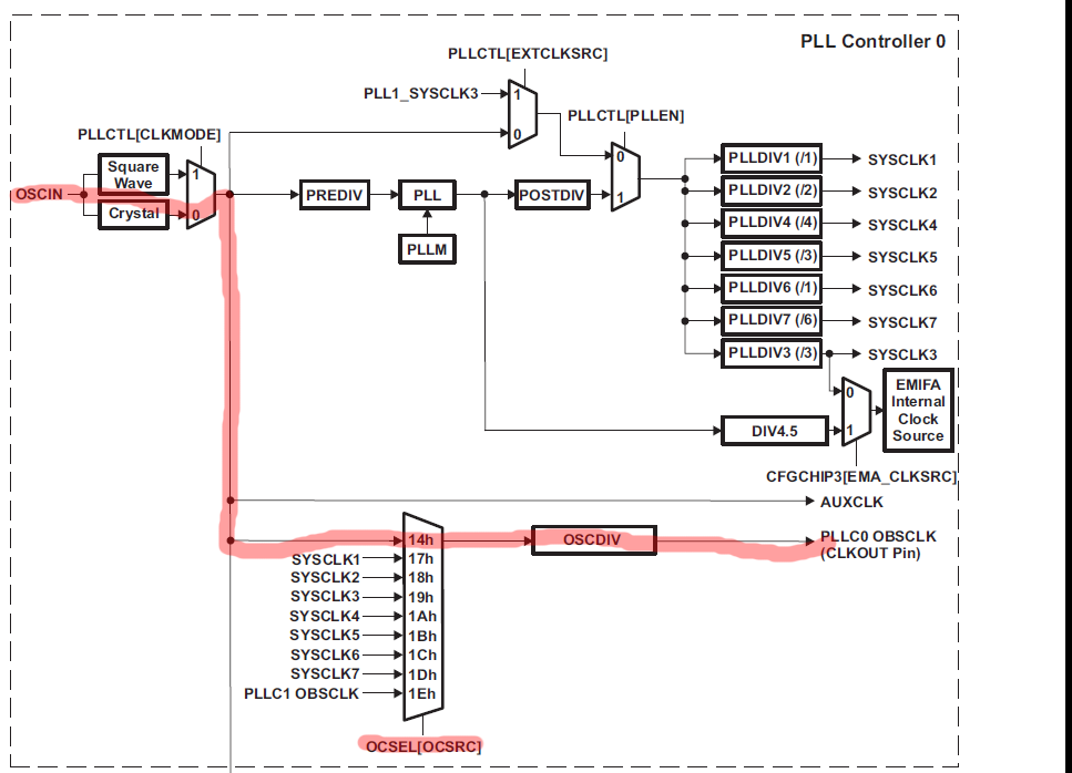
for clock PLL0 it is running by default with 300MHZ & PLL1 at 150MHZ as internal Oscilator is selected .

I am unable understand how the parameters like div,mul ,pre,post div are able config the clock for PLL0 and PLL1.

When I am trying see the clock by XCLKOUT pin by configuring as  clock out pin it is showing only 24MHZ(which is external crystal frequency).

Can any one tell me the formulae applying on it & how much is internal oscillator frequency?

Regards,

Ashrumochan.

  • Hi Ashrumochan,

    I think the spreadsheet available from this wiki will help you to understand the PLL parameters: processors.wiki.ti.com/.../AM18xx

    Check out the GEL file that is included with the CCS Target Configuration for C6748. There will be an example of the PLL initialization that you can play around with. Try generating new values with the spreadsheet, plugging them into the GEL file, and observing the CLKOUT frequency.

    Essentially CLKIN is pre-divided before the PLL to a slower clock frequency. Then the PLL uses the multiplier value to increase the frequency by the specified multiple. And then the post divider reduces the frequency coming out of the PLL.

    Refer also to CH7 Phase-Locked Loop Controller (PLLC) in the TRM: SPRUH79.

    You may need to configure the CLKOUT pin to output the SYSCLK you expect to see. It also has a divider feature before the CLKOUT pin.

    Hope this helps,
    Mark
  • In fact, the OBSCLK has a mux that defaults to select the input clock. This might explain why you see CLKIN at the CLKOUT pin. Use the Mux select to select a different clock like SYSCLK1.

    Regards,
    Mark

  • Hi Mark,

    Thanks for your kind information.

    I am configuring Xclockout pin correctly as you mentioned,Still I am unable to see the exact 300 Mhz as per example projects.

    Regards,

    Ashru

  • Hi Ashru,

    See these threads...

    e2e.ti.com/.../1817607
    e2e.ti.com/.../877072
    e2e.ti.com/.../1134332

    Can you verify that you are probing the CLKOUT at TP10 on the LCDK?
    The signal name is CLKOUT/PRU1_R30[13]/GP6[14]UHPI_HDS2

    Make sure you have configured the CLKOUT pinmux: the PINMUX13_7_4 bitfield in the PINMUX13 register (bits 7-4) needs to be set to 1h to select CLKOUT

    There are PLL0 and PLL1 registers, make sure you are using PLL0 registers.

    PLL0 Registers
    01C1 1104h OCSEL PLLC0 OBSCLK Select Register
    01C1 1124h OSCDIV PLLC0 Oscillator Divider 1 Register
    01C1 1148h CKEN PLLC0 Clock Enable Control Register

    PLL1 Registers
    01E1 A104h OCSEL PLLC1 OBSCLK Select Register
    01E1 A124h OSCDIV PLLC1 Oscillator Divider 1 Register
    01E1 A148h CKEN PLLC1 Clock Enable Control Register

    For OBSCLK to toggle, both the OD1EN bit in the OSCDIV register and the OBSEN bit in the CKEN register must be set to 1.

    Set OCSEL for PLL0 to SYSCLK1
    PLL0 OCSEL[OCSRC] = 17h SYSCLK1

    Note: To tap the PLL1 clocks, OCSEL for PLL0 must be set to 1Eh, and then the OCSEL for PLL1 selects the clock to route to CLKOUT.
    PLL0 OCSEL[OCSRC] = 1Eh PLLC1 OBSCLK

    Regards,
    Mark

  • Thanks mark,

    For giving me much clarity on the issue.

    Regards,

    Ashru