This thread has been locked.

If you have a related question, please click the "Ask a related question" button in the top right corner. The newly created question will be automatically linked to this question.

TMS320C6678: DDR3 clock frequency

Part Number: TMS320C6678

Hi,

How to calculate DDR3 clock speed?

I noticed CLK = CLKIN × ((PLLM+1) ÷ ((OUTPUT_DIVIDE+1) × (PLLD+1))) from datasheet section 2.5.4. So we can use that equation to calculate DDR3 clock speed right? I concluded from GEL file.

pdk_c667x_2_0_11\packages\ti\platform\evmc6678l

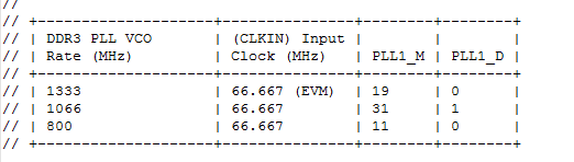
What i am confused is that the figure 7-23 in datasheet in which there is no need to add 1 with PLLM and PLLD. Please help to analyze in detail. 

By the way, what's VCO?

  • Nancy,

    The equation CLK = CLKIN × ((PLLM+1) ÷ ((OUTPUT_DIVIDE+1) × (PLLD+1))) is correct.  PLLM, OUTPUT_DIVIDE and PLLD are actual register bitfields that contain the value 1 less that the actual divider so that all values can be used including 0.  Also, in C6678, OUTPUT_DIVIDE is always 1.  The figure below from the DM is an oversimplification.

    It does not show the VCO (Voltage Controlled Oscillator) that is the core of the PLL (Phase Locked Loop).  The reference clock divider PLLD and the VCO output divider PLLM provide the structure for the PLL to control the VCO which generates a predictable frequency based on these values.  The OUTPUT_DIVIDER that divides the VCO clock by 2 to provide the PLLOUT clock rate.  The equation above provides the PLLOUT frequency.  Note that this clock is buffered through the PHY and becomes the signal on the DDRCLKOUTP/N pins which is driven to the SDRAMs.  The DDR data rate is twice the DDRCLKOUT signal. That is why the text in the GEL file shown in your post equates the VCO rate to the DDR data rate.

    Please refer to the KeyStone Architecture Phase-Locked Loop (PLL) User's Guide (SPRUGV2) for a more detailed discussion on the operation if the PLLs in the C6678.

    Tom