This thread has been locked.

If you have a related question, please click the "Ask a related question" button in the top right corner. The newly created question will be automatically linked to this question.

CCS/TMS320C6652: SPI boot failure

Part Number: TMS320C6652

Tool/software: Code Composer Studio

Hi,

I 'm trying to boot by SPI from nor flash directly.

This direct SPI firmware worked fine on the C6657EVM, then We created our custom board.

And, I modified this FW for C6652, and could load it with "No Boot" mode, this is working permanently.

Next step, I burned the FW to nor flash on our custom board. I confirmed that correct data were burned on the flash on my FW(using nor flash reading funtion).

I switched boot mode to "SPI Boot" mode, and I confirmed that C6652 was certainly driven as "SPI Boot" mode.

However, C6652 didn't boot. I already checked as follow.

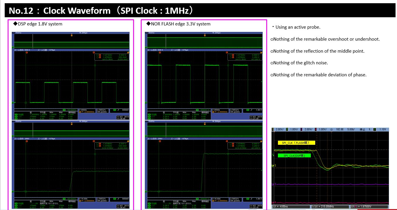
1. "SPI interfaces" signal integrity is good.

2. MISO line seems to receive data from flash device, but CS0 doesn't go up forever.

3. nysh.spi.map configuration is no problem, I think. please confirm the attached.

4. I updated parameter of DDR3 Configuration in the "emif4Cfg" structure. Please confirme the attached.

I don't understand why CS couldn't be going up.

What is the cause?

*c6652_board.c is loaded as board initialization. I recognize that this configuration is same as "emif4cfg". Is It correct?

Best regards,

#include <ti/csl/csl_bootcfgAux.h>
#include <ti/csl/cslr_device.h>
#include <ti/csl/csl_xmcAux.h>
#include <ti/csl/csl_emif4fAux.h>
#include <ti/csl/hw_types.h>

#include "board_internal.h"

extern void BOARD_delay(uint32_t usecs);

static void xmc_add_emif_cfg_region()
{
    /* mapping for ddr emif registers XMPAX*2 */
    CSL_XMC_XMPAXL    mpaxl;
    CSL_XMC_XMPAXH    mpaxh;

    /* base addr + seg size (64KB)*/    //"1B"-->"B" by xj */
    mpaxh.bAddr     = (0x2100000B >> 12);
    mpaxh.segSize   = (0x2100000B & 0x0000001F);

    /* replacement addr + perm*/
    mpaxl.rAddr     = 0x100000;
    mpaxl.sr        = 1;
    mpaxl.sw        = 1;
    mpaxl.sx        = 1;
    mpaxl.ur        = 1;
    mpaxl.uw        = 1;
    mpaxl.ux        = 1;

    /* set the xmpax for index2 */
    CSL_XMC_setXMPAXH(2, &mpaxh);
    CSL_XMC_setXMPAXL(2, &mpaxl);
}

/* Set the desired DDR3 configuration -- assumes 66.67 MHz DDR3 clock input */
Board_STATUS Board_DDR3Init()
{
    Board_STATUS             status = BOARD_SOK;
    uint32_t                 ddr3config, ddrPhyCtrl;
    uint8_t                  ddrPHYReadLatency;
    EMIF4F_TIMING1_CONFIG    sdram_tim1;
    EMIF4F_TIMING2_CONFIG    sdram_tim2;
    EMIF4F_TIMING3_CONFIG    sdram_tim3;
    EMIF4F_OUTPUT_IMP_CONFIG zqcfg;
    EMIF4F_PWR_MGMT_CONFIG   pwrmgmtcfg;
    EMIF4F_SDRAM_CONFIG      sdramcfg;

    xmc_add_emif_cfg_region();

    CSL_BootCfgUnlockKicker();

    /**************** 3.3 Leveling Register Configuration ********************/
    CSL_BootCfgGetDDRConfig(0, &ddr3config);
    ddr3config &= ~(0x007FE000);  // clear ctrl_slave_ratio field
    CSL_BootCfgSetDDRConfig(0, ddr3config);

    CSL_BootCfgGetDDRConfig(0, &ddr3config);
    ddr3config |= 0x00200000;     // set ctrl_slave_ratio to 0x100
    CSL_BootCfgSetDDRConfig(0, ddr3config);

    CSL_BootCfgGetDDRConfig(12, &ddr3config);
    ddr3config |= 0x08000000;    // Set invert_clkout = 1
    CSL_BootCfgSetDDRConfig(12, ddr3config);

    CSL_BootCfgGetDDRConfig(0, &ddr3config);
    ddr3config |= 0xF;            // set dll_lock_diff to 15
    CSL_BootCfgSetDDRConfig(0, ddr3config);

    CSL_BootCfgGetDDRConfig(23, &ddr3config);
    ddr3config |= 0x00000200;    // See section 4.2.1, set for partial automatic levelling
    CSL_BootCfgSetDDRConfig(23, ddr3config);

    /**************** 3.3 Partial Automatic Leveling ********************/
    if(DSP_DEVICE == EVM_C6657){
        ddr3config = 0x00;
        CSL_BootCfgSetDDRConfig(2,  ddr3config);
        ddr3config = 0x00;
        CSL_BootCfgSetDDRConfig(3,  ddr3config);
        ddr3config = 0x00;
        CSL_BootCfgSetDDRConfig(4,  ddr3config);
        ddr3config = 0x00;
        CSL_BootCfgSetDDRConfig(5,  ddr3config);
        ddr3config = 0x00;
        CSL_BootCfgSetDDRConfig(14,  ddr3config);
        ddr3config = 0x00;
        CSL_BootCfgSetDDRConfig(15,  ddr3config);
        ddr3config = 0x00;
        CSL_BootCfgSetDDRConfig(16,  ddr3config);
        ddr3config = 0x00;
        CSL_BootCfgSetDDRConfig(17,  ddr3config);
    } else if(DSP_DEVICE == C6652){
        ddr3config = 0x64;
        CSL_BootCfgSetDDRConfig(2,  ddr3config);
        ddr3config = 0x62;
        CSL_BootCfgSetDDRConfig(3,  ddr3config);
        ddr3config = 0x52;
        CSL_BootCfgSetDDRConfig(4,  ddr3config);
        ddr3config = 0x52;
        CSL_BootCfgSetDDRConfig(5,  ddr3config);
        ddr3config = 0x7E;
        CSL_BootCfgSetDDRConfig(14,  ddr3config);
        ddr3config = 0x81;
        CSL_BootCfgSetDDRConfig(15,  ddr3config);
        ddr3config = 0x75;
        CSL_BootCfgSetDDRConfig(16,  ddr3config);
        ddr3config = 0x75;
        CSL_BootCfgSetDDRConfig(17,  ddr3config);
    } else{
        ddr3config = 0x00;
        CSL_BootCfgSetDDRConfig(2,  ddr3config);
        ddr3config = 0x00;
        CSL_BootCfgSetDDRConfig(3,  ddr3config);
        ddr3config = 0x00;
        CSL_BootCfgSetDDRConfig(4,  ddr3config);
        ddr3config = 0x00;
        CSL_BootCfgSetDDRConfig(5,  ddr3config);
        ddr3config = 0x00;
        CSL_BootCfgSetDDRConfig(14,  ddr3config);
        ddr3config = 0x00;
        CSL_BootCfgSetDDRConfig(15,  ddr3config);
        ddr3config = 0x00;
        CSL_BootCfgSetDDRConfig(16,  ddr3config);
        ddr3config = 0x00;
        CSL_BootCfgSetDDRConfig(17,  ddr3config);
    }
    ddr3config = 0x00000033;
    CSL_BootCfgSetDDRConfig(6,  ddr3config);
    ddr3config = 0x0000003A;
    CSL_BootCfgSetDDRConfig(7,  ddr3config);
    ddr3config = 0x0000002C;
    CSL_BootCfgSetDDRConfig(8,  ddr3config);
    ddr3config = 0x0000002C;
    CSL_BootCfgSetDDRConfig(9,  ddr3config);
    ddr3config = 0x0000001C;
    CSL_BootCfgSetDDRConfig(10, ddr3config);
    ddr3config = 0x000000B7;
    CSL_BootCfgSetDDRConfig(18,  ddr3config);
    ddr3config = 0x000000B1;
    CSL_BootCfgSetDDRConfig(19,  ddr3config);
    ddr3config = 0x000000A4;
    CSL_BootCfgSetDDRConfig(20,  ddr3config);
    ddr3config = 0x000000A4;
    CSL_BootCfgSetDDRConfig(21,  ddr3config);
    ddr3config = 0x00000098;
    CSL_BootCfgSetDDRConfig(22,  ddr3config);

    /* Correct DQS-DQ write timing offset */
    ddr3config = 0x01000000;
    CSL_BootCfgSetDDRConfig(1,  ddr3config);

    /*Do a PHY reset. Toggle DDR_PHY_CTRL_1 bit 15 0->1->0 */
    CSL_EMIF4F_GetPhyControl(&ddrPhyCtrl, &ddrPHYReadLatency);
    ddrPhyCtrl &= ~(0x00008000);
    CSL_EMIF4F_SetPhyControl(ddrPhyCtrl, ddrPHYReadLatency);

    CSL_EMIF4F_GetPhyControl(&ddrPhyCtrl, &ddrPHYReadLatency);
    ddrPhyCtrl |= (0x00008000);
    CSL_EMIF4F_SetPhyControl(ddrPhyCtrl, ddrPHYReadLatency);

    CSL_EMIF4F_GetPhyControl(&ddrPhyCtrl, &ddrPHYReadLatency);
    ddrPhyCtrl &= ~(0x00008000);
    CSL_EMIF4F_SetPhyControl(ddrPhyCtrl, ddrPHYReadLatency);

    /***************** 3.4 Basic Controller and DRAM configuration ************/
    /* enable configuration */
    /*    hEmif->SDRAM_REF_CTRL    = 0x00006180; */
    uint32_t refresh_Rate = 0x00;
    CSL_EMIF4F_EnableInitRefresh();
    if(DSP_DEVICE == EVM_C6657){
        refresh_Rate = 0x515C;
    } else if(DSP_DEVICE == C6652){
        refresh_Rate = 0x0000411A;
    } else{
        refresh_Rate = 0x515C;
    }
    CSL_EMIF4F_SetRefreshRate(refresh_Rate);


    if(DSP_DEVICE == EVM_C6657){
        /*    hEmif->SDRAM_TIM_2   = 0x40877FEC; */
        sdram_tim1.t_wtr    = 4;
        sdram_tim1.t_rrd    = 1;
        sdram_tim1.t_rc     = 0x20;
        sdram_tim1.t_ras    = 0x17;
        sdram_tim1.t_wr     = 0x09;
        sdram_tim1.t_rcd    = 0x09;
        sdram_tim1.t_rp     = 0x09;
        /*    hEmif->SDRAM_TIM_2   = 0x40877FEC; */
        sdram_tim2.t_cke    = 3;
        sdram_tim2.t_rtp    = 4;
        sdram_tim2.t_xsrd   = 0x1FF;
        sdram_tim2.t_xsnr   = 0x071;
        sdram_tim2.t_xp     = 3;
        sdram_tim2.t_odt    = 0;
        /*    hEmif->SDRAM_TIM_3   = 0x55BF87FF; */
        sdram_tim3.t_rasMax     = 0xF;
        sdram_tim3.t_rfc        = 0x06A;
        sdram_tim3.t_tdqsckmax  = 0;
        sdram_tim3.zq_zqcs      = 0x3F;
        sdram_tim3.t_ckesr      = 4;
        sdram_tim3.t_csta       = 0x5;
        sdram_tim3.t_pdll_ul    = 0x5;
    } else if(DSP_DEVICE == C6652){
        sdram_tim1.t_wtr    = 0x03;
        sdram_tim1.t_rrd    = 0x03;
        sdram_tim1.t_rc     = 0x19;
        sdram_tim1.t_ras    = 0x12;
        sdram_tim1.t_wr     = 0x07;
        sdram_tim1.t_rcd    = 0x07;
        sdram_tim1.t_rp     = 0x07;
        sdram_tim2.t_cke    = 0x02;
        sdram_tim2.t_rtp    = 0x03;
        sdram_tim2.t_xsrd   = 0x1FF;
        sdram_tim2.t_xsnr   = 0x5A;
        sdram_tim2.t_xp     = 0x03;
        sdram_tim2.t_odt    = 0x00;
        sdram_tim3.t_rasMax     = 0x12;
        sdram_tim3.t_rfc        = 0x55;
        sdram_tim3.t_tdqsckmax  = 0x000;
        sdram_tim3.zq_zqcs      = 0x3F;
        sdram_tim3.t_ckesr      = 0x03;
        sdram_tim3.t_csta       = 0x05;
        sdram_tim3.t_pdll_ul    = 0x05;
    } else{
        sdram_tim1.t_wtr    = 4;
        sdram_tim1.t_rrd    = 1;
        sdram_tim1.t_rc     = 0x20;
        sdram_tim1.t_ras    = 0x17;
        sdram_tim1.t_wr     = 0x09;
        sdram_tim1.t_rcd    = 0x09;
        sdram_tim1.t_rp     = 0x09;
        sdram_tim2.t_cke    = 3;
        sdram_tim2.t_rtp    = 4;
        sdram_tim2.t_xsrd   = 0x1FF;
        sdram_tim2.t_xsnr   = 0x071;
        sdram_tim2.t_xp     = 3;
        sdram_tim2.t_odt    = 0;
        sdram_tim3.t_rasMax     = 0xF;
        sdram_tim3.t_rfc        = 0x06A;
        sdram_tim3.t_tdqsckmax  = 0;
        sdram_tim3.zq_zqcs      = 0x3F;
        sdram_tim3.t_ckesr      = 4;
        sdram_tim3.t_csta       = 0x5;
        sdram_tim3.t_pdll_ul    = 0x5;
    }

    CSL_EMIF4F_SetTiming1Config(&sdram_tim1);
    CSL_EMIF4F_SetTiming2Config(&sdram_tim2);
    CSL_EMIF4F_SetTiming3Config(&sdram_tim3);

    /*    hEmif->DDR_PHY_CTRL_1   = 0x0010010F; */
    ddrPHYReadLatency       = 0x0F;
    ddrPhyCtrl          = (0x0010010F);
    CSL_EMIF4F_SetPhyControl(ddrPhyCtrl, ddrPHYReadLatency);

    /*    hEmif->ZQ_CONFIG        = 0x70074C1F; */
    zqcfg.zqRefInterval     = 0x4C1F;
    zqcfg.zqZQCLMult        = 3;
    zqcfg.zqZQCLInterval    = 1;
    zqcfg.zqSFEXITEn        = 1;
    zqcfg.zqDualCSEn        = 1;
    zqcfg.zqCS0En           = 1;
    zqcfg.zqCS1En           = 0;
    CSL_EMIF4F_SetOutputImpedanceConfig(&zqcfg);

    /*    hEmif->PWR_MGMT_CTRL    = 0x0; */
    pwrmgmtcfg.csTime       = 0;
    pwrmgmtcfg.srTime       = 0;
    pwrmgmtcfg.lpMode       = 0;
    pwrmgmtcfg.dpdEnable    = 0;
    pwrmgmtcfg.pdTime       = 0;
    CSL_EMIF4F_SetPowerMgmtConfig(&pwrmgmtcfg);

    /* New value with DYN_ODT disabled and SDRAM_DRIVE = RZQ/7 */
    /*    hEmif->SDRAM_CONFIG     = 0x63077AB3; */
    CSL_EMIF4F_GetSDRAMConfig (&sdramcfg);

    if(DSP_DEVICE == EVM_C6657){
        sdramcfg.pageSize           = 2;
        sdramcfg.eBank              = 0;
        sdramcfg.iBank              = 3;
        sdramcfg.rowSize            = 5;
        sdramcfg.CASLatency         = 14;
        sdramcfg.narrowMode         = 1;
        sdramcfg.CASWriteLat        = 3;
        sdramcfg.SDRAMDrive         = 1;
        sdramcfg.disableDLL         = 0;
        sdramcfg.dynODT             = 2;
        sdramcfg.ddrDDQS            = 0;
        sdramcfg.ddrTerm            = 2;
        sdramcfg.iBankPos           = 0;
        sdramcfg.type               = 3;
    } else if(DSP_DEVICE == C6652){
        sdramcfg.pageSize           = 0x02;
        sdramcfg.eBank              = 0x00;
        sdramcfg.iBank              = 0x03;
        sdramcfg.rowSize            = 0x05;
        sdramcfg.CASLatency         = 0x06;
        sdramcfg.narrowMode         = 0x01;
        sdramcfg.CASWriteLat        = 0x01;
        sdramcfg.SDRAMDrive         = 0x01;
        sdramcfg.disableDLL         = 0x00;
        sdramcfg.dynODT             = 0x00;
        sdramcfg.ddrDDQS            = 0x00;
        sdramcfg.ddrTerm            = 0x03;
        sdramcfg.iBankPos           = 0x00;
        sdramcfg.type               = 0x03;
    } else{
        sdramcfg.pageSize           = 2;
        sdramcfg.eBank              = 0;
        sdramcfg.iBank              = 3;
        sdramcfg.rowSize            = 5;
        sdramcfg.CASLatency         = 14;
        sdramcfg.narrowMode         = 1;
        sdramcfg.CASWriteLat        = 3;
        sdramcfg.SDRAMDrive         = 1;
        sdramcfg.disableDLL         = 0;
        sdramcfg.dynODT             = 2;
        sdramcfg.ddrDDQS            = 0;
        sdramcfg.ddrTerm            = 2;
        sdramcfg.iBankPos           = 0;
        sdramcfg.type               = 3;
    }

    CSL_EMIF4F_SetSDRAMConfig(&sdramcfg);

    BOARD_delay(600); /*Wait 600us for HW init to complete*/

    /* Refresh rate = (7.8*666MHz] */
    /*    hEmif->SDRAM_REF_CTRL   = 0x0000144F;     */
    CSL_EMIF4F_EnableInitRefresh();
    if(DSP_DEVICE == EVM_C6657){
        refresh_Rate = 0x0000144F;
    } else if(DSP_DEVICE == C6652){
        refresh_Rate = 0x00001046;
    } else{
        refresh_Rate = 0x0000144F;
    }
    CSL_EMIF4F_SetRefreshRate(refresh_Rate);

    /***************** 4.2.1 Partial automatic leveling ************/
    /*    hEmif->RDWR_LVL_RMP_CTRL      =  0x80000000; */
    CSL_EMIF4F_SetLevelingRampControlInfo(1, 0, 0, 0, 0);

    /* Trigger full leveling - This ignores read DQS leveling result and uses ratio forced value */
    /*    hEmif->RDWR_LVL_CTRL          =  0x80000000; */
    CSL_EMIF4F_SetLevelingControlInfo(1, 0, 0, 0, 0);

    /************************************************************
      Wait for min 1048576 DDR clock cycles for leveling to complete
      = 1048576 * 1.5ns = 1572864ns = 1.57ms.
      Actual time = ~10-15 ms
     **************************************************************/
    BOARD_delay(3000); //Wait 3ms for leveling to complete

    return status;
}


#pragma  DATA_SECTION (emif4Cfg, ".emif4Cfg")
#pragma RETAIN (emif4Cfg)
const BOOT_EMIF4_TBL_T  emif4Cfg =  {

    BOOT_EMIF4_ENABLE_MSW_pllCtl          | \
    BOOT_EMIF4_ENABLE_MSW_sdRamTiming1    | \
    BOOT_EMIF4_ENABLE_MSW_sdRamTiming2    | \
    BOOT_EMIF4_ENABLE_MSW_sdRamTiming3    | \
    BOOT_EMIF4_ENABLE_MSW_ddrPhyCtl1      | \
    BOOT_EMIF4_ENABLE_MSW_sdRamRefreshCtl | \
	BOOT_EMIF4_ENABLE_MSW_sdRamOutImpdedCalCfg | \
	BOOT_EMIF4_ENABLE_MSW_sdRamConfig,

    BOOT_EMIF_ENABLE_SLSW_config0 | \
	BOOT_EMIF_ENABLE_SLSW_config6 | \
	BOOT_EMIF_ENABLE_SLSW_config7 | \
	BOOT_EMIF_ENABLE_SLSW_config8 | \
	BOOT_EMIF_ENABLE_SLSW_config9 | \
	BOOT_EMIF_ENABLE_SLSW_config10 | \
	BOOT_EMIF_ENABLE_SLSW_config18 | \
	BOOT_EMIF_ENABLE_SLSW_config19 | \
	BOOT_EMIF_ENABLE_SLSW_config20 | \
	BOOT_EMIF_ENABLE_SLSW_config22 | \
	BOOT_EMIF_ENABLE_SLSW_config12 | \
	BOOT_EMIF_ENABLE_SLSW_config23 | \
	BOOT_EMIF_ENABLE_SLSW_config21,      /* Config select slsw */
    0,      /* Config select lsw  */
    
    3,      /* pllPrediv  */
    64,     /* pllMult    */
    2,      /* pllPostDiv */

    0x63055AB2,//0x62477AB2,  /* sdRamConfig */
    0,           /* sdRamConfig2, dont care*/
    0x0000144F,//0x0000144F,  /* sdRamRefreshCtl  */
    0x0EEF265B,//0x1333780C,  /* sdRamTiming1 */
    0x305A7FDA,//0x30717FE3,  /* sdRamTiming2 */
    0x557F855F,//0x559F86AF,  /* sdRamTiming3 */

    0,           /* lpDdrNvmTiming, dont care */
    0,           /* powerManageCtl, dont care */
    0,           /* iODFTTestLogic, dont care */
    0,           /* performCountCfg, dont care */
    0,           /* performCountMstRegSel, dont care */
    0,           /* readIdleCtl, dont care */
    0,           /* sysVbusmIntEnSet, dont care */
    0x70074c1f,  /* sdRamOutImpdedCalCfg, dont care */
    0,           /* tempAlterCfg, dont care */

    0x0010010F,  /* ddrPhyCtl1 */

    0,           /* ddrPhyCtl2, dont care */
    0,           /* priClassSvceMap, dont care */
    0,           /* mstId2ClsSvce1Map, dont care */
    0,           /* mstId2ClsSvce2Map, dont care */
    0,           /* eccCtl, dont care */
    0,           /* eccRange1, dont care */
    0,           /* eccRange2, dont care */
    0,           /* rdWrtExcThresh, dont care */

    0x87A0047F, 0, 0, 0, 0, 0, 0x33, 0x3A,
    0x2C, 0x2C, 0x21, 0, 0xAF00002, 0, 0, 0,
    0, 0, 0xB7, 0xB1, 0xA4, 0xA4, 0x98, 0x200,
    0, 0, 0, 0, 0, 0, 0, 0,
    
    0, 0, 0, 0, 0, 0, 0, 0,
    0, 0, 0, 0, 0, 0, 0, 0,
    0, 0, 0, 0, 0, 0, 0, 0,
    0, 0, 0, 0, 0, 0, 0, 0
};

section {
 boot_mode = 50
 param_index = 0
 options = 1
 core_freq_mhz = 600
 exe_file = "spiboot.i2c.ccs"
 next_dev_addr_ext = 0x0
 sw_pll_prediv = 1
 sw_pll_mult = 12
 sw_pll_postdiv = 2
 sw_pll_flags = 1
 addr_width = 24
 n_pins = 4
 csel = 0
 mode = 0
 c2t_delay = 4
 bus_freq_mhz = 0
 bus_freq_khz = 500
}

  • Hi,

    1. Please ensure that the DEVSTAT register values are correct for SPI boot.

    2. Please ensure that the clock settings for the custom board is correct.

    3. Check the PC while the board fails to boot.

    4. Please ensure the DDR configuration values are programmed correctly.

    5.  You can look at the below example which is very straight forward to use.

    Note: We have C6657 direct SPI boot example in the following link which does not need c665x_board.c file.  Please user guide document under the docs directory.

  • Hi, Raja

    Thank you for your support.

    >>1. Please ensure that the DEVSTAT register values are correct for SPI boot.
    This is correct because Loading .gel file, .gel file recognized bootmode = 6(spiboot) .

    >>2. Please ensure that the clock settings for the custom board is correct.
    We will use C6652 with 600MHz core clock. and, this configuration is same as nysh.spi.map.
    We confirmed that "No boot" mode worked fine with loading the .gel file which set as 600MHz.

    >>3. Check the PC while the board fails to boot.
    I'm sorry that I Couldn't understand what this mean. How we check the PC?

    >>4. Please ensure the DDR configuration values are programmed correctly.
    I configured the DDR3 setting in the "emif4Cfg" structure. this is put at "DDR_CFG (RWX) : org = 0x8ffd20, len = 0x178" place.
    "C6657 EVM SPI boot example with DDR initialization " was helpful for this, and configuration parameters are same as them in the .gel.
    Those parameters are maybe no problem because We already confirmed that "No boot" mode.

    >>5. You can look at the below example which is very straight forward to use.
    I already used this example, and confirmed that C6657 on EVM worked fine(directly SPI boot).
    However C6652 on our custom board didn't work.

    We measured SPI interface with a oscilloscope as booting.
    As the results, our custom board and EVM are very similar. Therefore, SPI boot seemed to work and read the FW from nor flash, however DSP actually didn't read the internal RAM correctly.

    Previous "emif4Cfg" had some errors. I already updated this(Write Leveling Registers Configuration was wrong), but I get same errors.

    Where is the wrong in my configuration ?
    What the difference configuration between C6652 and C6657 except difference of DDR3 configuration ?


    Best regards,
  • Hi, Raja

    I attached the last updated DDR3 Configuration for the boot.


    const BOOT_EMIF4_TBL_T emif4Cfg = {

    BOOT_EMIF4_ENABLE_MSW_pllCtl | \
    BOOT_EMIF4_ENABLE_MSW_sdRamTiming1 | \
    BOOT_EMIF4_ENABLE_MSW_sdRamTiming2 | \
    BOOT_EMIF4_ENABLE_MSW_sdRamTiming3 | \
    BOOT_EMIF4_ENABLE_MSW_ddrPhyCtl1 | \
    BOOT_EMIF4_ENABLE_MSW_sdRamRefreshCtl | \
    BOOT_EMIF4_ENABLE_MSW_sdRamOutImpdedCalCfg | \
    BOOT_EMIF4_ENABLE_MSW_sdRamConfig,

    BOOT_EMIF_ENABLE_SLSW_config0 | \
    BOOT_EMIF_ENABLE_SLSW_config6 | \
    BOOT_EMIF_ENABLE_SLSW_config7 | \
    BOOT_EMIF_ENABLE_SLSW_config8 | \
    BOOT_EMIF_ENABLE_SLSW_config9 | \
    BOOT_EMIF_ENABLE_SLSW_config10 | \
    BOOT_EMIF_ENABLE_SLSW_config18 | \
    BOOT_EMIF_ENABLE_SLSW_config19 | \
    BOOT_EMIF_ENABLE_SLSW_config20 | \
    BOOT_EMIF_ENABLE_SLSW_config22 | \
    BOOT_EMIF_ENABLE_SLSW_config12 | \
    BOOT_EMIF_ENABLE_SLSW_config23 | \
    BOOT_EMIF_ENABLE_SLSW_config21, /* Config select slsw */
    0, /* Config select lsw */

    3, /* pllPrediv */
    64, /* pllMult */
    2, /* pllPostDiv */

    0x63055AB2,//0x62477AB2, /* sdRamConfig */
    0, /* sdRamConfig2, dont care*/
    0x0000411A,//0x0000144F, /* sdRamRefreshCtl */
    0x0EEF265B,//0x1333780C, /* sdRamTiming1 */
    0x305A7FDA,//0x30717FE3, /* sdRamTiming2 */
    0x557F855F,//0x559F86AF, /* sdRamTiming3 */

    0, /* lpDdrNvmTiming, dont care */
    0, /* powerManageCtl, dont care */
    0, /* iODFTTestLogic, dont care */
    0, /* performCountCfg, dont care */
    0, /* performCountMstRegSel, dont care */
    0, /* readIdleCtl, dont care */
    0, /* sysVbusmIntEnSet, dont care */
    0x70074c1f, /* sdRamOutImpdedCalCfg, dont care */
    0, /* tempAlterCfg, dont care */

    0x0010010F, /* ddrPhyCtl1 */

    0, /* ddrPhyCtl2, dont care */
    0, /* priClassSvceMap, dont care */
    0, /* mstId2ClsSvce1Map, dont care */
    0, /* mstId2ClsSvce2Map, dont care */
    0, /* eccCtl, dont care */
    0, /* eccRange1, dont care */
    0, /* eccRange2, dont care */
    0, /* rdWrtExcThresh, dont care */

    /* DDR3_CONFIG */
    0x87A0007F,//0x87A0047F, /* DDR3_CONFIG0 */
    0, /* not defined */
    0x64,//0, /* DDR3_CONFIG2 */
    0x62,//0, /* DDR3_CONFIG3 */
    0x52,//0, /* DDR3_CONFIG4 */
    0x52,//0, /* DDR3_CONFIG5 */
    0,//0x33, /* DDR3_CONFIG6 */
    0,//0x3A, /* DDR3_CONFIG7 */
    0,//0x2C, /* DDR3_CONFIG8 */
    0,//0x2C, /* DDR3_CONFIG9 */
    0,//0x21, /* DDR3_CONFIG10 */
    0, /* notdefined */
    0x08000000,//0x0xAF00002, /* DDR3_CONFIG12 */
    0, /* not defined */
    0x7E,//0, /* DDR3_CONFIG14 */
    0x81,//0, /* DDR3_CONFIG15 */
    0x75,//0, /* DDR3_CONFIG16 */
    0x75,//0, /* DDR3_CONFIG17 */
    0,//0xB7, /* DDR3_CONFIG18 */
    0,//0xB1, /* DDR3_CONFIG19 */
    0,//0xA4, /* DDR3_CONFIG20 */
    0,//0xA4, /* DDR3_CONFIG21 */
    0,//0x98, /* DDR3_CONFIG22 */
    0x200, /* DDR3_CONFIG23 */
    0, /* DDR3_CONFIG24 */

    0, 0, 0, 0, 0, 0, 0,

    0, 0, 0, 0, 0, 0, 0, 0,
    0, 0, 0, 0, 0, 0, 0, 0,
    0, 0, 0, 0, 0, 0, 0, 0,
    0, 0, 0, 0, 0, 0, 0, 0
    };

    .gel file was not updated. Please review that.
    SDTIM1~3, SDRFC configuration are suitable to our DDR3 using.

    Best regards,
  • Hi, Raja,

    >>3. Check the PC while the board fails to boot.
    I could understand that means what.
    I connected to the target when DSP booting.
    Then, pointing to 0x20B11B54 address. this is probably Boot Rom field, and it seemed to fail to boot with some reason.
    I don't know what 0x20B11B54 means.

    Please give me information as you can.

    Best, regards
  • I do not see any issues with sequence / procedure you have followed. 

    1. I recommend you to eliminate the DDR from boot sequence and try loading the code to internal MSMC from SPI.

    2. Is the reference clock used in your custom board and EVM are set the same frequency?

    3. Are you using the same Flash writer on EVM & Custom board? 

    Thank you.

  • Hi Raja,

    >>1. I recommend you to eliminate the DDR from boot sequence and try loading the code to internal MSMC from SPI.
    After I varied program, and confirmed to work from "No boot" mode, then I wrote it to nor flash.
    No matter whether I eliminated DDR3 configuration from a memory or didn't,
    as the result, SPI Boot always stops at 0x20B0EB90. I couldn't reproduce the previous status.

    >>2. Is the reference clock used in your custom board and EVM are set the same frequency?
    Yes, I confirmed that DSP received 100MHz freq for core PLL, and 50MHz freq for DDR3 PLL.
    However, C6652 is limited to 600MHz so that I configured that.

    >>3. Are you using the same Flash writer on EVM & Custom board?
    Yes, I use Nor Writer project which is provided TI.
    On the EVM, used flash is N25Q32A11ESE40F but we use MT25QL128ABA1EN7.
    The only difference between these devices is total block size because both of these are Micron devices.
    Actually, I could read and write while DSP is running as "No boot" mode.
    However, on my application program, I created my own because provided driver didn't work my project, and provided platform lib is to verbose(for multipurpose) for our application.
    Therefore, my program is customized completely for MT25QL128ABA1EN7, but Nor Writer project using platform lib without change. However, our program is contained in N25Q32A11ESE40F range, currently so I use Nor Writer project without change.

    Best regards,
  • As per the ROM map file the location 0x20b0eb90 is occupied by the function hw_spi_xfer.

    1. Please compare the spi scratch buff with your first 1KB of boot image at following location. Please provide the log as well here,

    008fa410   _spi_scratch_buf   size : 0x800

    2. We need to look at Binary dump at :

    008ffa80   _bootLog                  size : 0x84

     3. Also, get boot param dump from the following location:

    BPARAM                008fff00   00000080  00000080  00000000  RWIX


    HW break point:

    Please find the bootrom source code at,

    http://processors.wiki.ti.com/index.php/Keystone_Device_Architecture#Keystone_ROM_Boot_Examples_and_Reference_code

    Connect to the CCS, Set the HW breakpoints to following address and see you are able to hit any of the breakpoints by debugging.

    20b0af44   _bootMainSpi

    20b0ea00   _hw_spi_xfer

    20b0ec10   _hwSpiRead 

    20b0c490   _bootExit


    Please monitor the contents of scratch buffer after every SPI read and correlate it with the boot data. On the scope does it indicate that ROM reads certain number of bytes? Other thing to check would be the mode setting in DEVSTAT. Does the phase polarity mode settings match between the two flash parts.

    Thank you.

  • Hi Raja,

    Thanks for your reply.
    Reporting the result as follow, please confirm it, and let me know if there is a defect.

    >>1. Please compare the spi scratch buff with your first 1KB of boot image at following location. Please provide the log as well here,
    I experimented three our custom boards with same firmware.
    Each of all, "_spi_scratch_buf" became different value among them, and different from written "app.dat" data.

    >>2. We need to look at Binary dump at : 008ffa80 _bootLog size : 0x84
    It indicated "00000000" NOP. what this means?

    >>3. 3. Also, get boot param dump from the following location: BPARAM 008fff00 00000080 00000080 00000000 RWIX
    "008fff00" indicated "00000028".

    I tried debugging with pointing 20b0af44, 20b0ea00, 20b0ec10, 20b0c490.
    Program went back and forth between 0x20b0ea00(_hw_spi_xfer) and 0x20b0ec10.
    confirmed the waveform, SPI MOSI and SPI MISO permanently were permanently reading and writing.
    This means that it couldn't arrive at _bootExit I think.
    devstat reg = 0001C40D(11100010000001101). this indicates that,
    - PCIESSEN = 0x1(C6654 Only)
    - PCIESSMODE = 0x11(C6654 Only)
    - BOOTMODE = 0x0001000000110(mode0, 4pin mode, 24bit addr, SPI BOOT)
    - LENDIAN = 0x1(Little)
    DEVSTAT has no problem.

    I noticed that MT25QL128ABA1EN7 and N25Q32A11ESE40F require the same READ & WRITE timing and it seems to require spi mode "3".
    When EVM booting, and when cusom application reading flash, spi mode was 0, but these worked fine.

    I can't understand what is correct.
    What is happening?

    Best regards,
  • Hi Raja,

    I'm sorry.
    I told you something that is not true.

    I told that I eliminated the DDR Configuration, however it probably wasn't eliminated.
    The obvious cause is at DDR Configuration in the "emif4Cfg".
    I noticed EVM(C6657) didn't work too when I mistook to write the our custom boards configuration to EVM(C6657).
    In this case, EVM was reading something data permanently like our custom boards.
    Therefore, there is probably something wrong at ddr configuration for our custom board.
    I configured that referring to .gel, but there is probably still wrong.

    Is it possible for spi to enter an infinite loop if the DDR settings are not correct?
    I want to check just in case.

    Best regards,
  • I told that I eliminated the DDR Configuration, however it probably wasn't eliminated.
    The obvious cause is at DDR Configuration in the "emif4Cfg".
    I noticed EVM(C6657) didn't work too when I mistook to write the our custom boards configuration to EVM(C6657).
    In this case, EVM was reading something data permanently like our custom boards.
    Therefore, there is probably something wrong at ddr configuration for our custom board.
    I configured that referring to .gel, but there is probably still wrong.

    Is it possible for spi to enter an infinite loop if the DDR settings are not correct?
    I want to check just in case.

    Thank you for the update. 

    Looks like there is some problem creating boot image in your setup. I remember, you were able to do spi direct boot in EVM. Have you tried with pre-built images from TI or your files? Is it possible for you to eliminate DDR from process as first step? 

    I hope you have followed the below note from document mentioned before. Please confirm (Docs\SPIboot_with_DDR_UserGuide.doc).

    Important Note: The romparse utility that is part of the SDK is designed to add boot address 0x51 in the boot parameter table appended to the boot image. Ensure that the value at 0x1F offset in the image is 00 and not 0x51

    Thank you.

  • Hi Raja,

    Thank you for your support.

    >>Looks like there is some problem creating boot image in your setup. I remember, you were able to do spi direct boot in EVM. Have you tried with pre-built images from TI or your files? Is it possible for you to eliminate DDR from process as first step?

    Yes, I succeeded to boot on the EVM with both of our FW and TI's. On the EVM, my latest FW worked(application is completely same as c6652 use).

    The other day, I eliminated the definition of emif4Cfg from FW so I thought I could eliminate the DDR configuration. I confirmed that emif4Cfg didn't exist in .map file.

    However I didn't change my platform file and memory section in it(I use RTSC project). In this case, is it correct to regard that the DDR configuration couldn't be eliminated?

    If I hope to eliminate it completely, should I change my platform file? How can I create the FW without DDR configuration?

    On the other hands, I checked the procedure to create the boot image in advance. Of course I referenced the user guide, and here is my .bat to create image.

    set IBL_UTIL=.\utils
    hex6x spiboot.rmd
    b2i2c spiboot.btbl spiboot.btbl.i2c
    b2ccs spiboot.btbl.i2c spiboot.i2c.ccs
    romparse nysh.spi.map
    copy i2crom.ccs spirom_le.dat
    byteswapccs i2crom.ccs spirom_le_swap.dat
    ccs2bin i2crom.ccs spirom_le.bin
    ccs2bin -swap i2crom.ccs spirom_le_swap.bin
    copy spirom_le_swap.dat ..\..\writer\nor\Debug\
    copy nor_writer_input.txt ..\..\writer\nor\Debug\
    pause

    I used nor writer project to burn the image, I loaded .dat on CCS, copied to DDR firstly and wrote to nor flash. It's a proven way to boot the EVM.

    I finally got spirom_le_swap.dat and manually changed 0x51 to 0x00. I could confirm it on debugging, memory browser indicates my boot parameters are correctly set.

    please review the attached.

    Even now I continue to investigate, I appreciate you to support.

    Best regards,

  • Hi Raja,

    This is added information.

    As booting from SPI directly, DEVSTAT = 0x1c40d.

    0x40d  indicates  BOOTMODE[12:0]. I recognized that this means "SPI boot mode".

    0x1C000 indicates PCIESSEN and PCIESSMODE[1:0] but these are need for C6654 Only.

    It seems that DSP sometimes doesn't stop at SPI xfer but stops at 0x20b11b54 or 0x20b11b50 or 0x20b11b56.

    I don't understand what is trigger of this change.  Are these pieces of information also a hint?

    Best regards,

  • However I didn't change my platform file and memory section in it(I use RTSC project). In this case, is it correct to regard that the DDR configuration couldn't be eliminated?

    If I hope to eliminate it completely, should I change my platform file? How can I create the FW without DDR configuration?

    TI provided direct boot example does not use the RTSC project. Update the cmd file to run from MSMC and build it. Thank you.

  •  It seems that DSP sometimes doesn't stop at SPI xfer but stops at 0x20b11b54 or 0x20b11b50 or 0x20b11b56.

    These locations are address of delay routines in boot ROM.

    Thank you.

  • Hi Raja,

    >>TI provided direct boot example does not use the RTSC project. Update the cmd file to run from MSMC and build it. Thank you.

    Ti example's linker.cmd

    MEMORY
    {
        DDR_CFG   :  origin = 0x8ffd20, length = 0x180
        L2MAGIC   :  origin = 0x8ffffc, length = 0x4

        DDR       :  origin = 0x80000000, length = 0x2000
    }


    SECTIONS
    {
        .emif4Cfg > DDR_CFG

        .stack > DDR
        .msmc  > DDR
        .data  > DDR
        .far   > DDR
        .text  > DDR
        .const > DDR
        .cinit > DDR
        .lmagic > L2MAGIC
       
    }

    My linker.cmd(C6652)

    MEMORY
    {
        L2SRAM (RWX) : org = 0x800000, len = 0xff000
        DDR_CFG (RWX) : org = 0x8ffd20, len = 0x178
        L2MAGIC (RWX) : org = 0x8ffffc, len = 0x4
        DDR3 (RWX) : org = 0x80000000, len = 0x20000000
    }

    SECTIONS
    {
        .text: load >> L2SRAM
        .ti.decompress: load > L2SRAM
        .stack: load > L2SRAM
        GROUP: load > L2SRAM
        {
            .bss:
            .neardata:
            .rodata:
        }
        .cinit: load > L2SRAM
        .pinit: load >> L2SRAM
        .init_array: load > L2SRAM
        .const: load >> L2SRAM
        .data: load >> L2SRAM
        .fardata: load >> L2SRAM
        .switch: load >> L2SRAM
        .sysmem: load > L2SRAM
        .far: load >> L2SRAM
        .args: load > L2SRAM align = 0x4, fill = 0 {_argsize = 0x0; }
        .cio: load >> L2SRAM
        .ti.handler_table: load > L2SRAM
        .c6xabi.exidx: load > L2SRAM
        .c6xabi.extab: load >> L2SRAM
        .vecs: load > L2SRAM
        xdc.meta: load > L2SRAM, type = COPY

    }

    My linker.cmd(C6657EVM)

    MEMORY
    {
        DDR_CFG (RWX) : org = 0x8ffd20, len = 0x178
        L2SRAM (RWX) : org = 0x800000, len = 0xff000
        L2MAGIC (RWX) : org = 0x8ffffc, len = 0x4
        MSMCSRAM (RWX) : org = 0xc000000, len = 0x100000
        DDR3 (RWX) : org = 0x80000000, len = 0x20000000
    }

    SECTIONS
    {
        .text: load >> L2SRAM
        .ti.decompress: load > L2SRAM
        .stack: load > L2SRAM
        GROUP: load > L2SRAM
        {
            .bss:
            .neardata:
            .rodata:
        }
        .cinit: load > L2SRAM
        .pinit: load >> L2SRAM
        .init_array: load > L2SRAM
        .const: load >> L2SRAM
        .data: load >> L2SRAM
        .fardata: load >> L2SRAM
        .switch: load >> L2SRAM
        .sysmem: load > L2SRAM
        .far: load >> L2SRAM
        .args: load > L2SRAM align = 0x4, fill = 0 {_argsize = 0x0; }
        .cio: load >> L2SRAM
        .ti.handler_table: load > L2SRAM
        .c6xabi.exidx: load > L2SRAM
        .c6xabi.extab: load >> L2SRAM
        .vecs: load > L2SRAM
        xdc.meta: load > L2SRAM, type = COPY

    }

    Our added manual cmd file(C6652,6657 common)

    SECTIONS
    {
        .emif4Cfg > DDR_CFG
        .init_array:     load >> L2SRAM
        .mcbsp:          load >> L2SRAM
        .mcbspSharedMem: load >> L2SRAM
         platform_lib:   load >> L2SRAM
         //systemHeap:     load >> L2SRAM
         systemHeap:     load >> DDR3
        .far:             load >> DDR3
        .fardata:         load >> DDR3
        .nor_flash         load >> DDR3
        .lmagic > L2MAGIC
    }

    The difference between C6657 and C6652 is only at section "MSMCSRAM (RWX) : org = 0xc000000, len = 0x100000",  C6657 is booted but C6652 is not booted.

    I confirmed that C6652's MSMC memory is assigned to Reserved from device manual. Also, platform file of RTSC generate platform model excluding this section.

    I gave it a try to add the ".msmc" section according to TI's but nothing change.

    Anyway, I can't understand how to indicate DSP to boot from MSMC.

    Sorry to bother you, please lecture me more details of configuration to boot from MSMC without DDR3.

  • Hi Raja,


    I think that has multiple problem as SPI communications.


    1. It doesn't work as spi mode 0 or 3.
    I confirmed that our using flash is compatible to spi mode 0 or 3.
    our using flash is MT25QL128ABA made by Micron and this device is upper compatible to N25Q032A(on EVM).
    However, changing spi mode to boot as spi mode 1 or 2, DSP correctly booted.
    Why does this happen? Both of those flash are compatible to same spi mode, nevertheless,  there is obvious difference to boot.

    2. About SPI CLK integrity
    At the begining, I told you that spi clock integrity is good and it seems that now I still think so, but probably clock waveform has something problem.
    If our hardware team implemented a capacitor or a damping resistor, changing spi mode to 1 or 2, DSP could boot.
    Influence of a capacitor or a damping resistor has the effect of delaying hold timing, however this effect applied only to clock line.
    Even if those implemented to MISO or MOSI, however hold timing is extended, boot is failure.

    Please confirm the attaced. This is our added investigation. give us your support.


    regards,

  • As booting from SPI directly, DEVSTAT = 0x1c40d.

    0x40d  indicates  BOOTMODE[12:0]. I recognized that this means "SPI boot mode".

    0x1C000 indicates PCIESSEN and PCIESSMODE[1:0] but these are need for C6654 Only.

    It seems that DSP sometimes doesn't stop at SPI xfer but stops at 0x20b11b54 or 0x20b11b50 or 0x20b11b56.

    I don't understand what is trigger of this change.  Are these pieces of information also a hint?

    Looking at the tables "Table 8-1. C6654 and C6652 Device Configuration Pins" and "Table 4-2. Terminal functions - Signals and Control by Function" from data manual, the PCIESSEN and PCIESSMODE setting comes from external configuration on the pins (W21,V21 and AD20) and there is an external pull down on the pins so the configuration could be a setting on their board as the ROM only reads these values and doesn`t write to this field. Is there an external pull up on their board for this configuration.


    The difference between C6657 and C6652 is only at section "MSMCSRAM (RWX) : org = 0xc000000, len = 0x100000",  C6657 is booted but C6652 is not booted.

    The changes to boot from internal memory is looking correct. Make sure that you have enough memory to load the sections on internal L2 or MSMC.

    Thank you.

  •  

    2. About SPI CLK integrity
    At the begining, I told you that spi clock integrity is good and it seems that now I still think so, but probably clock waveform has something problem.
    If our hardware team implemented a capacitor or a damping resistor, changing spi mode to 1 or 2, DSP could boot.
    Influence of a capacitor or a damping resistor has the effect of delaying hold timing, however this effect applied only to clock line.
    Even if those implemented to MISO or MOSI, however hold timing is extended, boot is failure.

    Please confirm the attaced. This is our added investigation. give us your support.

    Here is the response from our hardware expert,

    I was not able to clearly determine whether this was a hardware issue or a software / configuration issue. Therefore, without understanding the root cause, I would not recommend adding a capacitor to the clock line as a solution.

    I believe he indicated that he could reliably write and read the FLASH from CCS. You need to make sure that this is clearly confirmed before moving on to the next part of debugging this issue. Also, compare the dump of PLL and SPI port configuration during this robust operation and its failing.

    Thank you.

  • Hi Raja,

    Thank you for new information.

    After our research, I probably understood what is cause.

    For SPI Controller in Keystone, general spi mode 0(adoptive to NOR flash too) means Keystone's spi mode 1.

    And our custom board's default boot strap status to be applicable spi mode is 00(this means Keystone's spi mode 0).

    On the other hands, Micron NOR flash is compatible to spi mode 0 or 3(Keystone's 1 or 2).

    Therefore, the sequence of DEVSTAT register probably work as the follow.

    Therefore I think that our custom boards are working as spec however doesn't understand why EVM work as above. this fact confuse me so much.

    regards,

  •  For SPI Controller in Keystone, general spi mode 0(adoptive to NOR flash too) means Keystone's spi mode 1. On the other hands, Micron NOR flash is compatible to spi mode 0 or 3(Keystone's 1 or 2).

    I am confused. As you said earlier, flash supports SPI mode 0 and 3 which is "Input data is latched on the falling edge of SPICLK" and in keystone also SPI mode 0 and 3 are same. Please look at below boot parameter table from C6652 data manual. 

  • Hi Raja,

    I report the final result of our research.

    >>I am confused. As you said earlier, flash supports SPI mode 0 and 3 which is "Input data is latched on the falling edge of SPICLK" and in keystone also SPI mode 0 and 3 are same.

    Please confirm my reply at Jun 12, 2019 1:47 PM.

    What I always say "general spi mode 0" is "Input data is latched on the rising edge of SPICLK". This is the common to Micron flash however, only TI device is different from this in this case.

    Actually, our hardware team confirmed that "TI's spi mode 1" works as "general spi mode 0" from its spi clk timing.

    One thing I couldn't understand yet is why "TI's spi mode 0" works with "general spi mode 0(Micron is compatible)" on the EVM.

    I consider that if working different mode for DSP, but being sufficient timing > 5ns, it works.

    On the EVM, It happened to be moving didn't it?

    regards,