This thread has been locked.

If you have a related question, please click the "Ask a related question" button in the top right corner. The newly created question will be automatically linked to this question.

AM3358: DDR3 access fail

Part Number: AM3358


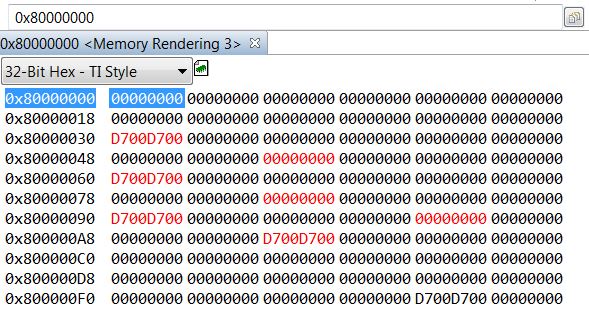
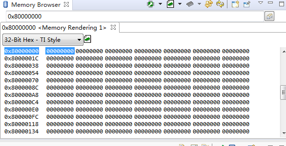
One customer's board. DDR access fail, tried from 400MHz, 300MHz, 303Mhz, to even 200MHz, 100MHz, memory display are 0. already configured timing and control register according to DDR datasheet.

replace different vendor's DDR device, same result, scanned with X-ray, solder is good.

Please give some advices how to debug the "brick"?

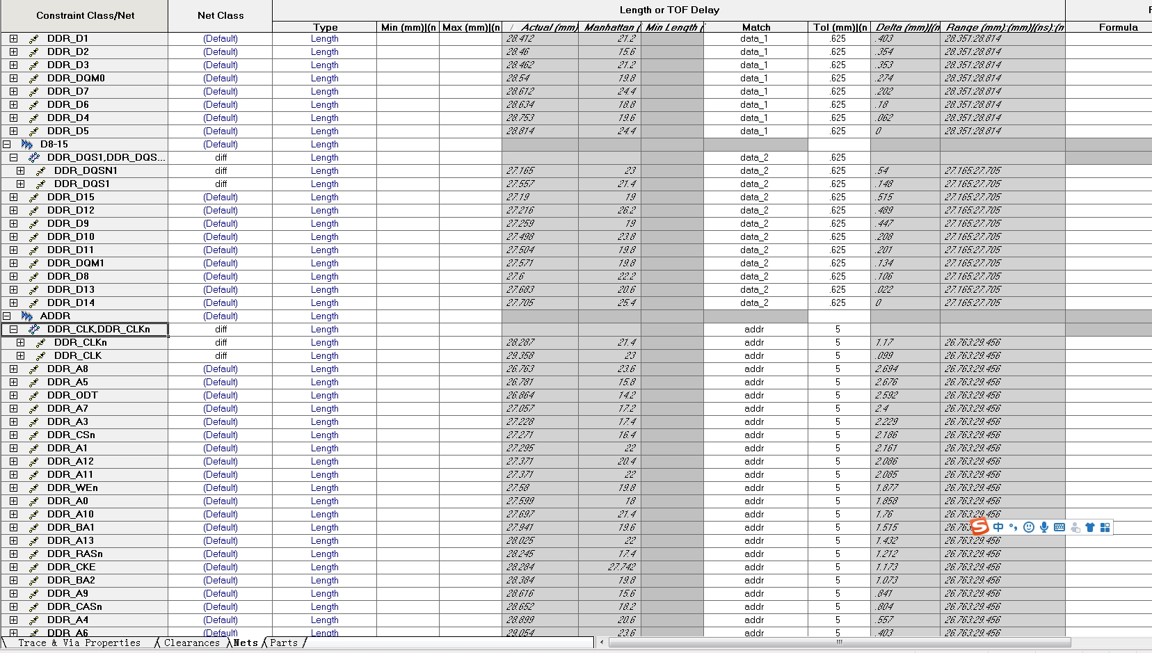
DDR3 layout data as below:

  • Would somebody help me. no matter how to change configuration. can't read/write success.

  • Tony, please send the customers Ratio Seed Spreadsheet and the AC Timing spreadsheet from the wiki: processors.wiki.ti.com/.../AM335x_DDR_PHY_register_configuration_for_DDR3_using_Software_Leveling

    Furthermore, have the customer run the ddr-analysis script from this page: git.ti.com/.../master
    Instruction can be found in the README file.

    What is the topology of the DDR3 design? What is the memory part number?

    Regard,s
    James
  • James,

    I can't download the tar ball, either git clone.DDR_configuration.zip

    DDR device: MT41J64M16-125

  • James,
    if possible, please share me the tools via BOX.
  • Tony, you should be able to just click on source tree to see the files.  The ddr-analysis.dss is just one file and the README is also there.

    Have your customer change PHY_INVERT_CLKOUT =1 and then make the appropriate changes in the source code

    Regards,

    James

  • James,

    Now I can and did it. It is a bit confuse to me. it mentioned not to use gel file to initialize target, then the target should be in default status.

    I attached the result, please help analysis.

    Skipping read of EMIF registers since EMIF clock disabled.
     * EMIF registers are not readable when in DS0 state
     * If you are attempting to enter DS0 this is normal.
    
    ************************
    *** IOCTRL Registers ***
    ************************
    
    CONTROL: DDR_CMD0_IOCTRL = 0x00000004
      * ddr_ba2 Pullup/Pulldown disabled
      * ddr_wen Pullup/Pulldown disabled
      * ddr_ba0 Pullup/Pulldown disabled
      * ddr_a5 Pullup/Pulldown disabled
      * ddr_ck Pullup/Pulldown disabled
      * ddr_ckn Pullup/Pulldown disabled
      * ddr_a3 Pullup/Pulldown disabled
      * ddr_a4 Pullup/Pulldown disabled
      * ddr_a8 Pullup/Pulldown disabled
      * ddr_a9 Pullup/Pulldown disabled
      * ddr_a6 Pullup/Pulldown disabled
      * Bits 9:5 control ddr_ck and ddr_ckn
        - Slew fastest
        - Drive Strength 5 mA
      * Bits 4:0 control ddr_ba0, ddr_ba2, ddr_wen, ddr_a[9:8], ddr_a[6:3]
        - Slew fastest
        - Drive Strength 9 mA
    CONTROL: DDR_CMD1_IOCTRL = 0x00000004
      * ddr_a15 Pullup/Pulldown disabled
      * ddr_a2 Pullup/Pulldown disabled
      * ddr_a12 Pullup/Pulldown disabled
      * ddr_a7 Pullup/Pulldown disabled
      * ddr_ba1 Pullup/Pulldown disabled
      * ddr_a10 Pullup/Pulldown disabled
      * ddr_a0 Pullup/Pulldown disabled
      * ddr_a11 Pullup/Pulldown disabled
      * ddr_casn Pullup/Pulldown disabled
      * ddr_rasn Pullup/Pulldown disabled
      * Bits 4:0 control ddr_15, ddr_a[12:10], ddr_a7, ddr_a2, ddr_a0, ddr_ba1, ddr_casn, ddr_rasn
        - Slew fastest
        - Drive Strength 9 mA
    CONTROL: DDR_CMD2_IOCTRL = 0x00000004
      * ddr_cke Pullup/Pulldown disabled
      * ddr_resetn Pullup/Pulldown disabled
      * ddr_odt Pullup/Pulldown disabled
      * ddr_a14 Pullup/Pulldown disabled
      * ddr_a13 Pullup/Pulldown disabled
      * ddr_csn0 Pullup/Pulldown disabled
      * ddr_a1 Pullup/Pulldown disabled
      * Bits 4:0 control ddr_cke, ddr_resetn, ddr_odt, ddr_csn0, ddr_[a14:13], ddr_a1
        - Slew fastest
        - Drive Strength 9 mA
    CONTROL: DDR_DATA0_IOCTRL = 0x00000004
      * ddr_d8 Pullup/Pulldown disabled
      * ddr_d9 Pullup/Pulldown disabled
      * ddr_d10 Pullup/Pulldown disabled
      * ddr_d11 Pullup/Pulldown disabled
      * ddr_d12 Pullup/Pulldown disabled
      * ddr_d13 Pullup/Pulldown disabled
      * ddr_d14 Pullup/Pulldown disabled
      * ddr_d15 Pullup/Pulldown disabled
      * ddr_dqm1 Pullup/Pulldown disabled
      * ddr_dqs1 and ddr_dqsn1 Pullup/Pulldown disabled
      * Bits 9:5 control ddr_dqs1, ddr_dqsn1
        - Slew fastest
        - Drive Strength 5 mA
      * Bits 4:0 control ddr_d[15:8], ddr_dqm1
        - Slew fastest
        - Drive Strength 9 mA
    CONTROL: DDR_DATA1_IOCTRL = 0x00000004
      * ddr_d0 Pullup/Pulldown disabled
      * ddr_d1 Pullup/Pulldown disabled
      * ddr_d2 Pullup/Pulldown disabled
      * ddr_d3 Pullup/Pulldown disabled
      * ddr_d4 Pullup/Pulldown disabled
      * ddr_d5 Pullup/Pulldown disabled
      * ddr_d6 Pullup/Pulldown disabled
      * ddr_d7 Pullup/Pulldown disabled
      * ddr_dqm0 Pullup/Pulldown disabled
      * ddr_dqs0 and ddr_dqsn0 Pullup/Pulldown disabled
      * Bits 9:5 control ddr_dqs0, ddr_dqsn0
        - Slew fastest
        - Drive Strength 5 mA
      * Bits 4:0 control ddr_d[7:0], dqm0
        - Slew fastest
        - Drive Strength 9 mA
    CONTROL: DDR_IO_CTRL = 0x00000000
      * Bit 31: DDR_RESETn controlled by EMIF.
      * Bit 28 (mddr_sel) configured for SSTL, i.e. DDR2/DDR3/DDR3L operation.
    CONTROL: VTP_CTRL = 0x00010107
      * VTP not disabled (expected in normal operation, but not DS0).
    CONTROL: VREF_CTRL = 0x00000000
      * VREF supplied externally (typical).
    CONTROL: DDR_CKE_CTRL = 0x00000000
      * CKE gated (forces pin low).
    

  • James,

    I use gel file initialize board, then disconnect JTAG, use script to dump register configuration. got output as attachment. I tried both 0 and 1  with CMD_PHY_INVERT_CLKOUT. no different to DDR behavior.

    Seems this script was designed to dump register file for checking, I think my configuration should be OK, and I helped many other customer's board DDR bring up before.

    Question: 

    #1. If inappropriate DDR layout, will it result in DDR read/write totally fail like a brick? 

    #2. From my experience, usually the value write in one address will display on other address. then use DDR leveling can adjust it. but to this board, it did not display on other address.

    CONTROL: device_id = 0x2b94402e
      * AM335x family
      * Silicon Revision 2.1
    
    CONTROL: control_status = 0x00400322
      * SYSBOOT[15:14] = 01b (24 MHz)
    CM_CLKSEL_DPLL_DDR = 0x00012f17
      * DPLL_MULT = 303 (x303)
      * DPLL_DIV = 23 (/24)
    CM_DIV_M2_DPLL_DDR = 0x00000201
      * CLKST = 1: M2 output clock enabled
      * DIVHS = 1 (/1)
    
    DPLL_DDR Summary
     -> F_input = 24 MHz
     -> CLKOUT_M2 = DDR_PLL_CLKOUT = 303 MHz
    
    EMIF: SDRAM_CONFIG = 0x61c05232
      * Bits 31:29 (reg_sdram_type) set for DDR3
      * Bits 28:27 (reg_ibank_pos) set to 0
      * Bits 26:24 (reg_ddr_term) set for RZQ/4 (001b)
      * Bits 22:21 (reg_dyn_odt) DDR3 dynamic ODT set to RZQ / 2
      * Bit  20    (reg_ddr_disable_dll) set to 0, DDR3 DLL enabled
      * Bits 19:18 (reg_sdram_drive) set for RZQ/6 (00b)
      * Bits 17:16 (reg_cwl) set for 0, CWL = 5
      * Bits 15:14 (reg_narrow_mode) set to 1 -> 16-bit EMIF interface
      * Bits 13:10 (reg_cl) set to 4 -> CL = 6
      * Bits 09:07 (reg_rowsize) set to 4 -> 13 row bits
      * Bits 06:04 (reg_ibank) set to 3 -> 8 banks
      * Bits 02:00 (reg_pagesize) set to 2 -> 10 column bits
    
    EMIF: PWR_MGMT_CTRL = 0x00000000
     * Bits 10:8 reg_lp_mode set to 0, auto power management disabled
     * Warning: Bits 7:4 (reg_sr_tim) are in violation of Maximum Self-Refresh Command Limit
       -> Please see the silicon errata (DDR3: JEDEC Compliance for Maximum Self-Refresh Command Limit) for more details.
       -> This is only an issue if used in conjunction with reg_lp_mode=2.
    
    DDR PHY: DDR_PHY_CTRL_1 = 0x00000007
      * WARNING: reg_phy_enable_dynamic_pwrdn disabled.
      * Bits 9:8 (reg_phy_rd_local_odt) to 0 -> no termination
        -> Read termination is highly recommended in general for best DDR3 signal integrity
      * Bits 4:0 (reg_read_latency) set to 7
        -> If PHY_INVERT_CLKOUT=0, this is an appropriate value.
        -> If PHY_INVERT_CLKOUT=1, this is too small.
        -> PHY_INVERT_CLKOUT is a write-only register, so this needs to be
        -> inspected closely in the code and RatioSeed spreadsheet.
    
    *********************
    *** Register Dump ***
    *********************
    
    *(0x4c000000) = 0x40443403
    *(0x4c000004) = 0x40000000
    *(0x4c000008) = 0x61c05232
    *(0x4c00000c) = 0x00000000
    *(0x4c000010) = 0x0000093b
    *(0x4c000014) = 0x0000093b
    *(0x4c000018) = 0x0888a39b
    *(0x4c00001c) = 0x0888a39b
    *(0x4c000020) = 0x2a247fda
    *(0x4c000024) = 0x2a247fda
    *(0x4c000028) = 0x501f821f
    *(0x4c00002c) = 0x501f821f
    *(0x4c000038) = 0x00000000
    *(0x4c00003c) = 0x00000000
    *(0x4c000054) = 0x00ffffff
    *(0x4c000058) = 0x8000140a
    *(0x4c00005c) = 0x00021616
    *(0x4c000080) = 0x00000000
    *(0x4c000084) = 0x00000000
    *(0x4c000088) = 0x00010000
    *(0x4c00008c) = 0x00000000
    *(0x4c000090) = 0x0934bd97
    *(0x4c000098) = 0x00050000
    *(0x4c00009c) = 0x00050000
    *(0x4c0000a4) = 0x00000000
    *(0x4c0000ac) = 0x00000000
    *(0x4c0000b4) = 0x00000000
    *(0x4c0000bc) = 0x00000000
    *(0x4c0000c8) = 0x50074be4
    *(0x4c0000d4) = 0x00000000
    *(0x4c0000d8) = 0x00000000
    *(0x4c0000dc) = 0x00000000
    *(0x4c0000e4) = 0x00000007
    *(0x4c0000e8) = 0x00000007
    *(0x4c000100) = 0x00000000
    *(0x4c000104) = 0x00000000
    *(0x4c000108) = 0x00000000
    *(0x4c000120) = 0x00000305
    
    ************************
    *** IOCTRL Registers ***
    ************************
    
    CONTROL: DDR_CMD0_IOCTRL = 0x0000018b
      * ddr_ba2 Pullup/Pulldown disabled
      * ddr_wen Pullup/Pulldown disabled
      * ddr_ba0 Pullup/Pulldown disabled
      * ddr_a5 Pullup/Pulldown disabled
      * ddr_ck Pullup/Pulldown disabled
      * ddr_ckn Pullup/Pulldown disabled
      * ddr_a3 Pullup/Pulldown disabled
      * ddr_a4 Pullup/Pulldown disabled
      * ddr_a8 Pullup/Pulldown disabled
      * ddr_a9 Pullup/Pulldown disabled
      * ddr_a6 Pullup/Pulldown disabled
      * Bits 9:5 control ddr_ck and ddr_ckn
        - Slew slow
        - Drive Strength 9 mA
      * Bits 4:0 control ddr_ba0, ddr_ba2, ddr_wen, ddr_a[9:8], ddr_a[6:3]
        - Slew slow
        - Drive Strength 8 mA
    CONTROL: DDR_CMD1_IOCTRL = 0x0000018b
      * ddr_a15 Pullup/Pulldown disabled
      * ddr_a2 Pullup/Pulldown disabled
      * ddr_a12 Pullup/Pulldown disabled
      * ddr_a7 Pullup/Pulldown disabled
      * ddr_ba1 Pullup/Pulldown disabled
      * ddr_a10 Pullup/Pulldown disabled
      * ddr_a0 Pullup/Pulldown disabled
      * ddr_a11 Pullup/Pulldown disabled
      * ddr_casn Pullup/Pulldown disabled
      * ddr_rasn Pullup/Pulldown disabled
      * Bits 4:0 control ddr_15, ddr_a[12:10], ddr_a7, ddr_a2, ddr_a0, ddr_ba1, ddr_casn, ddr_rasn
        - Slew slow
        - Drive Strength 8 mA
    CONTROL: DDR_CMD2_IOCTRL = 0x0000018b
      * ddr_cke Pullup/Pulldown disabled
      * ddr_resetn Pullup/Pulldown disabled
      * ddr_odt Pullup/Pulldown disabled
      * ddr_a14 Pullup/Pulldown disabled
      * ddr_a13 Pullup/Pulldown disabled
      * ddr_csn0 Pullup/Pulldown disabled
      * ddr_a1 Pullup/Pulldown disabled
      * Bits 4:0 control ddr_cke, ddr_resetn, ddr_odt, ddr_csn0, ddr_[a14:13], ddr_a1
        - Slew slow
        - Drive Strength 8 mA
    CONTROL: DDR_DATA0_IOCTRL = 0x0000018b
      * ddr_d8 Pullup/Pulldown disabled
      * ddr_d9 Pullup/Pulldown disabled
      * ddr_d10 Pullup/Pulldown disabled
      * ddr_d11 Pullup/Pulldown disabled
      * ddr_d12 Pullup/Pulldown disabled
      * ddr_d13 Pullup/Pulldown disabled
      * ddr_d14 Pullup/Pulldown disabled
      * ddr_d15 Pullup/Pulldown disabled
      * ddr_dqm1 Pullup/Pulldown disabled
      * ddr_dqs1 and ddr_dqsn1 Pullup/Pulldown disabled
      * Bits 9:5 control ddr_dqs1, ddr_dqsn1
        - Slew slow
        - Drive Strength 9 mA
      * Bits 4:0 control ddr_d[15:8], ddr_dqm1
        - Slew slow
        - Drive Strength 8 mA
    CONTROL: DDR_DATA1_IOCTRL = 0x0000018b
      * ddr_d0 Pullup/Pulldown disabled
      * ddr_d1 Pullup/Pulldown disabled
      * ddr_d2 Pullup/Pulldown disabled
      * ddr_d3 Pullup/Pulldown disabled
      * ddr_d4 Pullup/Pulldown disabled
      * ddr_d5 Pullup/Pulldown disabled
      * ddr_d6 Pullup/Pulldown disabled
      * ddr_d7 Pullup/Pulldown disabled
      * ddr_dqm0 Pullup/Pulldown disabled
      * ddr_dqs0 and ddr_dqsn0 Pullup/Pulldown disabled
      * Bits 9:5 control ddr_dqs0, ddr_dqsn0
        - Slew slow
        - Drive Strength 9 mA
      * Bits 4:0 control ddr_d[7:0], dqm0
        - Slew slow
        - Drive Strength 8 mA
    CONTROL: DDR_IO_CTRL = 0x00000000
      * Bit 31: DDR_RESETn controlled by EMIF.
      * Bit 28 (mddr_sel) configured for SSTL, i.e. DDR2/DDR3/DDR3L operation.
    CONTROL: VTP_CTRL = 0x00010167
      * VTP not disabled (expected in normal operation, but not DS0).
    CONTROL: VREF_CTRL = 0x00000000
      * VREF supplied externally (typical).
    CONTROL: DDR_CKE_CTRL = 0x00000001
      * CKE controlled by EMIF (normal/ungated operation).
    

  • Tony, what software are they using to configure the DDR.  Did they start with a GEL file, or go straight to modifying a bootloader.  Can they send us the code that is used to configure DDR, especially all of the DDR PHY registers?

    Yes, an inappropriate layout can result in all kinds of issues.  Let's first ensure their software configuration is correct.  Once we can confirm the configuration,  then we can look at possible h/w issues.

    Also, how many boards are failing?

    Regards,

    james 

  • AM335x_HP.gel

    MICRON-MT41J64M16.pdf

    use gel file, MT41J64M16.

    customer made 4 pcs boards, same result. I got one on hand for debugging, no matter how to adjust timing, CL, DDR frequency, CPU frequency, no much change on DDR behavior.

  • An offline conference call revealed that the customer has accidentally swapped RAS and CAS signals on the schematic.

    Regards,

    James