This thread has been locked.

If you have a related question, please click the "Ask a related question" button in the top right corner. The newly created question will be automatically linked to this question.

66AK2G12: CHIP BEAD needed for TPS65911A GNDA_PMIC/GDNREF ?

Part Number: 66AK2G12

Hi,

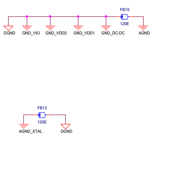
My customer is considering to use registers rather than chip beads on TPS65911A GNDA_PMIC/GDNREF. Please take a look at the EVM schematic :

Our PMIC FAE is saying this is not specific requirements for TPS65911A . So I posted the questions here. Could you clarify the reason for using chip beads ?

Best Regards,
NK

  • Hi,

    Could you please specify which K2G EVM schematics are you referring to: GP EVM or ICE?

    ICE does not use a PMIC, and the K2G EVM uses TPS659118.

    Best Regards,

    Yordan

  • Hello, Yordan.

    Sorry for the confusion. The snapshot I've attached in the previous post is from the customer's schematic. Here is from K2GEVM (SPRR302.pdf):

    They refereed EVM schematic for their custom board. As you see, TPS659118 is in the EVM schematic, but because they are using 66AK2G12(1Ghz) on their custom board, their PMIC is not TPS659118, but TPS65911A. They have followed this TPS659118 schematic design for their TPS65911A.

    Best Regards,
    NK

  • Hi Naoki,

    I couldn't find a specific requirement in the user guides or K2G datasheet. I believe the ferrite beads were added to reduce EMI interference (but I could be missing something).

    Anyway I included the design team to elaborate on this.

    Best Regards,
    Yordan

  • Hi Naoki,

    The TPS659118 switching supply circuits result in large AC current loops. We attempt to keep the ground plane associated with these loops local to the power supply circuit to provide large currents flowing on the rest of the power plane. Some layouts will provide a cut-out around the power supply ground with a small neck connection to the ground plane. We have attempted this in the past but the cutout is often lost when revisions are made to the PCB since all the ground connections are the same in the schematic. By adding the small filter component it forces the PCB designer to keep that portion of the ground plane isolated. The filter is not a requirement, just a convenience when completing the PCB design.

    Regards, Bill

  • Hi Bill

    Thank you for your reply. I got some additional questions from the customer;

    It seems the beads are needed to separate GND from the other planes in order to prevent form flowing big current. I understand the beads is not specific requirement for K2G/PMIC design, but in the first place, what is the actual intention for that ? I'm wondering if you wanted to control the potential problems which might be caused by the current flow. Or, was that your general design policy ?  Do you have any comment on this ? And please let me know if you have verified the K2G/PMIC operation without the beads on PMIC. 

    Best Regards,
    NK

  • Hi Naoki,

    First let me qualify my answer and say that I am not an expert in power supply design. The link below provides a very good post on switching power supply design and has a good diagram showing the different current loops associated with those power supplies.

    http://blog.optimumdesign.com/switching-power-supply-pcb-layout-considerations-towards-a-better-switcher

    I have found that most layout guidelines for switching power supplies attempt to keep the power supply and the associated passive components on the same side of the board along with the ground plane for the AC current loop. That local ground plane is connected to the internal digital ground plane with vias, usually off to one side of the local plane. This is difficult to achieve with PMIC components since it usually includes multiple power supplies. As I explained in the previous post, adding the filter component allows us to establish a local ground plane on an inner layer and forces the PCB designer to keep that ground separate from digital ground plane. We have not verified the K2G EVM without the local ground plane, that would require a different layout for the board. 

    Regards, Bill

  • Hello Bill,

    Thank you very much for your answer. I got some feedback from the customer:

    Yes, I understood that chip beads was helpful to create a small current loop in case of PMIC use case (It has multiple power supplies).
    I would like to have your comments about the beads impedance and its side effect. EVM`s beads have 150Ω~180Ω impedance at the range of 200~1000MHz. Here, the separated GND was actually for DVDD33_USB and DVDD18.  Considering our USB use case (relatively higher data rate), this impedance might cause problems like voltage drop in the system. What do you think of this ? Could you please suggest ?

    Best Regards,
    NK

  • Hi Naoki,

    The impedance of the bead might cause some issue with the proper operation of the PMIC but I don't think that the data rate of the USB would have any result in any issues. If the customer is concerned with the impedance of the bead, it could be replaced with a zero ohm resistor or with vias to the common ground plane. We have not seen any issues with the design as delivered so we haven't made any changes.

    Regards, Bill

  • Hello Bill,

    Thanks for your answers. My customer would re-consider about their design based on your suggestions.

    Best Regards,
    NK